Photo above: Simulation of the future Fab38 in Kiryat Gat, Israel
Israel’s Government and Intel have reached an agreement to expand Intel’s Fab38 in Kiryat Gat, approximately 40 Km from Gaza, where it has an existing chip plant (Fab28). Intel Israel announced an expantion plan of $15 billion in Fab38 planned to be completed within 4-5 years. It will bring the total investment in this fab to $25 billion and enable it to produce advanced semiconductors based on Extreme ultraviolet (EUV) lithography process.
The government of Israel will grant Intel with $3.2 billion worth of incentives. The new fab is expected to create thousands new jobs and to have a major role Intel’s global IDM 2.0 strategy. Intel Israel was founded in 1974 in Haifa, as Intel’s first development center outside the USA, and in 1981 the first factory outside the USA was established in Jerusalem. Today, Intel Israel is the largest private employer in the Israeli hi-tech sector with 11,700 direct employees plus additional 42,000 in indirect employment.
Along with its leading manufacturing facility In Kiryat Gat, Intel operates three development centers in Haifa, Petah Tikva and Jerusalem, focused mainly on the development of new Processors, Connectivity and Networking technologies, Artificial Intelligence and Cyber Security solutions. During 2022 Intel Israel’s export totalled $8.7 billion representing 5.5% of the hi-tech exports from Israel.
In an interview with Fox Business last week, Intel CEO, Pat Gelsinger, talked about Intel’s employees during the current Israel-Hamas war. He said: “Many Intel employees in Israel died on October 7, some are being held hostage still in Gaza, and a great many are on reserve duty. But Israelis are the most resilient people on earth. They have not missed a single commitment despite the conflict. That’s why we believe so deeply in them.”
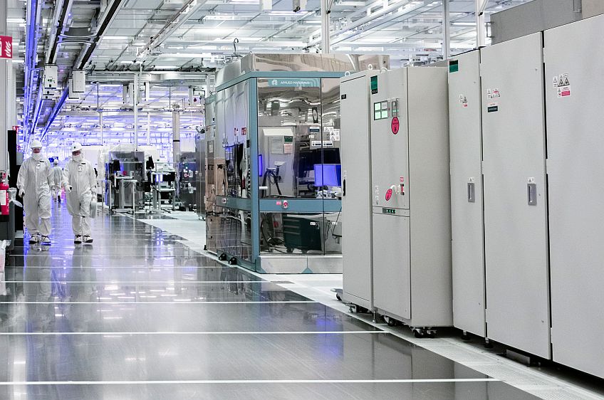
Photo above: Intel’s Fab 34 in Leixlip, Ireland. $200 million for each EUV Lithography machine
In March 2021, Intel embraced the IDM 2.0 strategy and established Intel Foundry Services as the strategic wing that leads multi-billion dollar in investments throughout Europe and the USA. When this move was first announced, it was seen as a direct threat to TSMC – the world’s largest semiconductor contract manufacturing services provider. This was mainly due to Pat Gelsinger, Intel’s CEO and the shaper of IDM 2.0 strategy, stating multiple times that Intel’s goal is to become the world’s most prominent manufacturing services provider.
The idea seemed unreasonable: why would a genuine semiconductor manufacturer who sells their own processors for high-profit margins shift to another business model – a manufacturing services provider with much lower profit margins? The investors also did not find the idea exciting. In March 2021, Intel’s shares were traded at $64 on NASDAQ. Currently, the shares are worth $35.5 with a market cap of $149 billion.
However, Techtime’s visit to Intel’s new factory in Ireland, Fab 34, reveals that the reason behind the new move is technological rather than merely business. To be more precise, the enormous cost of shifting to advanced manufacturing processes.
€17 billion and five years to set up
Last week, Intel inaugurated Fab 34 in Leixlip, Ireland, which brings Intel 4 technology (equivalent to 7nm) to Europe. It is also the first use of EUV (Extreme Ultraviolet) technology in high-volume manufacturing (HVM) in Europe. The construction of the new fab had began in 2019 and had required €17 billion investments. To provide a point of comparison, Intel operates 3 more fabs in its Leixlip campus that use older technologies, and these factories cost a combined total of €13 billion.
It means that building a fab with the latest technology, such as EUV lithography machines, would be a significant financial undertaking. Industry experts suggest that a factory like this would require 10-20 EUV lithography machines, which are only produced by the Dutch company ASML. Each EUV lithography system costs approximately $200 million.
Inside Fab 34 in Leixlip, Ireland. Credit: Intel
The construction of the new factory demands using novell chemical materials for the production of RibbonFET transistors, acquiring new and spcialized equipment and process control and measurements, and a significantly larger clean room that meets higher standards. It is improbable that a single company that bears these expenses and only sells its own products would be able to market them at a profitable price. This is why there are only three companies toady active in advanced processes chips: Samsung, TSMC, and Intel. GlobalFoundries was the last independent firm to be involved in this competition, but it withdrew in 2018.
Intel follows Samsung’s model
Samsung, who acknowledged this challenge earlier, developed a business model for producing self-designed chips together with providing manufacturing services to its competitors, such as Apple and Qualcomm. There are also other companies that embraced this approach, although they are not taking part in the advanced technology race. French STMicroelectronics, for instance, has also adopted this approach by balancing production costs by providing manufacturing services to clients like Mobileye.
Intel’s recent move leaves TSMC as the only company solely focused on providing manufacturing services. Currently, TSMC is the primary supplier of advanced chips to Intel’s largest competitors, including AMD and Nvidia. The conclusion is that Intel’s business model does not pose a threat to TSMC, and there is no indication that Intel intends to compete with TSMC. In fact, Intel has taken significant measures to mitigate the risks associated with transitioning to advanced manufacturing processes.
This is crucial if Intel wants to maintain its position as a market leader. During the recent inauguration ceremony in Ireland, Dr. Ann Kelleher, Intel’s VP and general manager of Technology Development, announced that the company is currently developing four new processes: Intel 3, Intel A20, Intel A18, and the cutting-edge Intel Next. Kelleher stated that the company’s goal is to achieve one trillion transistors in a chip by 2030.
Chiplets require an Open Production Floor
The financial revolution is being accelerated by the move towards hybrid components that consist of several Chiplets; each produced using a different process. This shift creates a new business model where modern processors no longer rely on a single CPU chip but instead integrate multiple peripheral chips from other manufacturers onto an advanced substrate that connects numerous tiles.
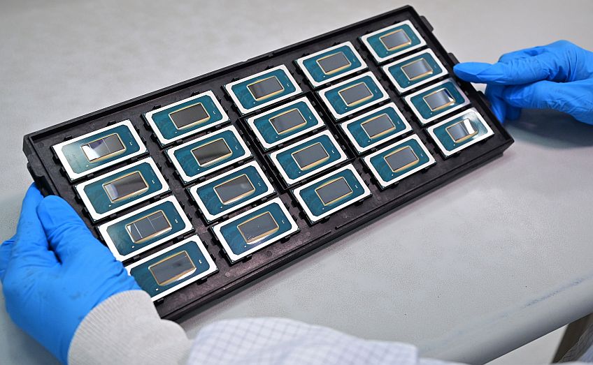
Intel’s Meteor Lake chips. 25% made by Intel, %75 by TSMC
This concept is similar to the IP Model prevalent in the Chip Design industry, where any SoC contains the manufacturer’s own proprietary module, along with multiple intellectual property (IP) modules designed by specialized firms. Adopting multi-tile components expands the IP model to the Hardware Level. But it requires to adjust the nature of production lines. Intel, for instance, utilizes this approach in its new chip, Meteor Lake, where 75% of the surface area of the silicon tiles is manufactured by TSMC, and only 25% by Intel.
This shift necessitates the management of an open production floor that can accommodate tiles produced by other manufacturers while producing their own. It also requires the integration of foreign silicon into Intel’s components and the transfer of Intel’s silicon into other vendors’ components, even if they are direct competitors. To achieve this, Intel appears to have chosen a production model that combines self-development and production, side by side with providing manufacturing services.
The Chinese model travels West
Fab 34 project also reveals the importance role of national governments in the semiconductor industry. The cost of transitioning to advanced processes is so high that even major companies like Intel require government incentives. Similar to the Chinese approach, public funding is used to support production firms and boost local industries that rely on advanced technology to create more jobs.
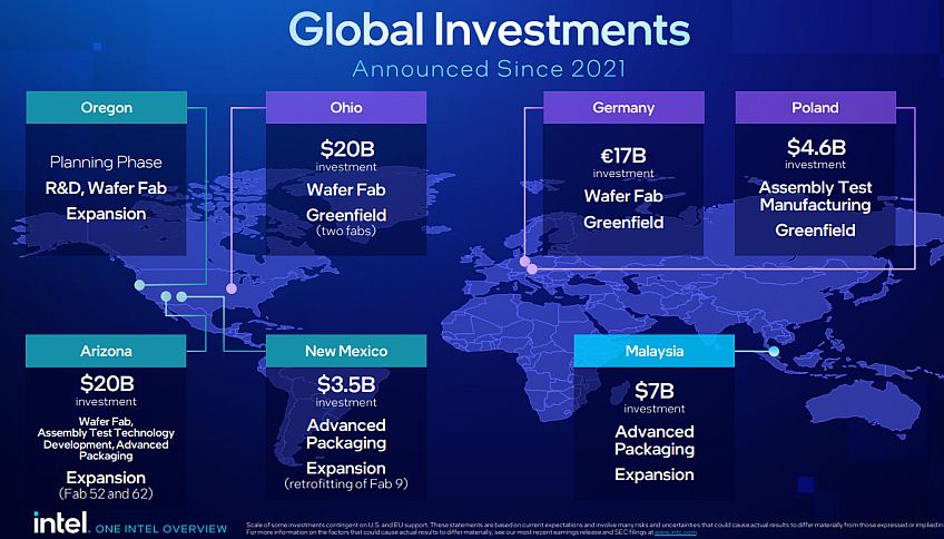
This is why countries like Ireland and Israel are appealing, and why the CHIPS Act and Science Act drive the build-up of new fabs in the US. Intel is also awaiting now to receive approvals from the EU before it will move to the construction phase of its next European fabs: A wafer fabrication facility in Magdeburg, Germany, and an assembly and test facility in Wrocław, Poland.
Photo above: Intel’s Fab 11X in Rio Rancho, New Mexico. Credit: Intel Inc.
Less than a month after the termination of a planned merger between Intel and Tower Seniconductor, the two companies announced a largescale production agreement: Intel will provide foundry services and 300mm manufacturing capacity to help Tower serve its customers globally. Tower will utilize Intel’s manufacturing facility in Rio Rancho, New Mexico (Fab 11X), and will invest up to $300 million to acquire and own equipment and other fixed assets to be installed in the facility.
The rearranement of the fab will provide production capacity of over 600,000 photo layers per month. Intel will manufacture Tower’s 65-nanometer power management BCD (bipolar-CMOS-DMOS) and radio frequency silicon on insulator (RF SOI) solutions flows. Stuart Pann, Intel senior vice president and general manager of Intel Foundry Services (IFS) explained during Goldman Sachs Communacopia & Technology Conference this week, that intel had unused capacity in Fab 11X, because it is an older factory for older technologies.
Initial Production in 2025
Pann: “We found a way to do contract manufacturing to take advantage of that extra space. Those older tools that we aren’t using, taking some investment from Tower to finish out the line.” The parties plan to achieve full process flow qualification in 2024, and to begin with full mass production in 2025. Tower CEO Russell Ellwanger said: “We see this collaboration as a first step towards multiple unique synergistic solutions with Intel.”
Tower provides foundry services for Analog semicinductor devices. It offers a broad range of customizable process platforms such as SiGe, BiCMOS, mixed-signal/CMOS, RF CMOS, CMOS image sensor, non-imaging sensors, integrated power management (BCD and 700V), and MEMS. Tower owns two manufacturing facilities in Israel (150mm and 200mm), two in the U.S. (200mm), two facilities in Japan (200mm and 300mm) which it owns through its 51% holdings in TPSCo and is sharing with ST a 300mm manufacturing facility in Italy .
After it had failed to recieve the needed approval of Chinese regulators, , Intel Corporation announced that it has mutually agreed with Tower Semiconductor to terminate its previously disclosed agreement to acquire Tower. On February 15, 2022 Intel and Tower Semiconductor announced a definitive agreement under which Intel will acquire Tower for $53 per share in cash, representing a total enterprise value of approximately $5.4 billion. The aimed to strenthen Intel’s IDM 2.0 strategy to become a leading chip production services provider (foundry).
But during the last 18 months, the US-China tension proved to be a stronger force than Intel’s ambitions, and even after the deal had received across the board approvals, the Chinese authorities made no effort to proceed, and actually waited until it will be clear that no approvel is expexted to be given in the near future. “Our respect for Tower has only grown through this process” said Pat Gelsinger, CEO of Intel, “and we will continue to look for opportunities to work together in the future.”
Russell Ellwanger, Tower Semiconductor CEO, said: “We appreciate the efforts by all parties. During the past 18 months, we’ve made significant technological, operational, and business advancements. We are well positioned to continue to drive our strategic priorities and short-, mid- and long-term tactics with a continued focus on top and bottom-line growth.”
Tower Semiconductor provides a broad range of customizable process platforms such as SiGe, BiCMOS, mixed-signal/CMOS, RF CMOS, CMOS image sensor, non-imaging sensors, integrated power management (BCD and 700V), and MEMS. It owns two manufacturing facilities in Israel (150mm and 200mm), two in the U.S. (200mm), three facilities in Japan (two 200mm and one 300mm) which it owns through its 51% holdings in TPSCo and is sharing a 300mm manufacturing facility being established in Italy with ST.
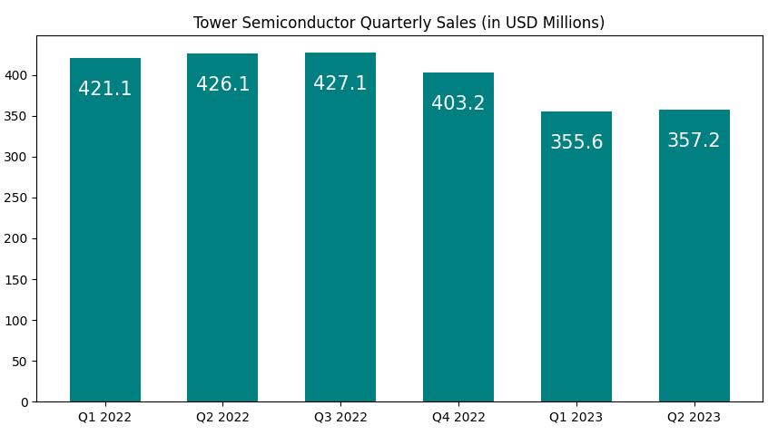
During the last year it faced a slight decline in sales, from $847 millions in H1 2022, to approximately $713 million in H1 2023. until this morning Tower was traded in NASDAQ in valuation of 3.85 billion – 20% below the deal valuation. It means that many investors preculated the deal will fail. Following the deal termination, Tower’s share lost additional 10%, bringing its valuation to approximately $3.5 billion
Intel announced that Shlomit Weiss, senior vice president and co-general manager (GM) of the Design Engineering Group (DEG), will replace senior vice president Sunil Shenoy, who will retire at the end of the year. Weiss will lead the company’s design, development, validation and manufacturing support of intellectual properties (IPs) and system-on-chips (SoCs), reporting directly to Intel CEO Pat Gelsinger and joining the company’s executive leadership team.
Weiss has spent 28 years at Intel in engineering and leadership roles, including as leader of cross-site teams responsible for IP and discrete data center products, and general manager of data center group silicon development. She played a major role in the development of some of Intel’s most successful processors, including Sandy Bridge (2006) and Sky Lake (2015). In 2017 she joined Mellanox, now part of Nvidia, as Senior VP for Silicon Engineering.
Last year Shlomit had returned to Intel as co-GM of DEG with Shenoy, specifically leading client product design engineering and the Intel architecture core portfolio used across client, data center and other segments. “The design engineering organization requires a leader with deep technical expertise and passion for engineering excellence, and Shlomit has that in spades,” Gelsinger said.
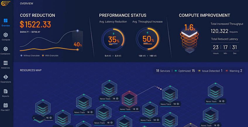
Intel Corporation announced an agreement to acquire Granulate Cloud Solutions, an Israel-based developer of real-time continuous optimization software. The acquisition of Granulate will help cloud and data center customers maximize compute workload performance and reduce infrastructure and cloud costs. Deal terms are not being disclosed, but it is expected to close in the second quarter of 2022. At that time, Granulate’s 120 employees will be integrated into Intel’s Datacenter and AI business unit.
Sandra Rivera, GM of the Datacenter and AI Group at Intel, said that Granulate’s autonomous optimization software can be applied to production workloads without the need to make changes in the customer’s code. Greg Lavender, GM of the Software and Advanced Technology Group at Intel, explained that Granulate’s real-time optimization software complements Intel’s capabilities by helping customers to gain performance and reduce Cloud costs.
How It Works
Granulate’s real-time continuous optimization is a new approach to optimizing production workloads by leveraging resource usage patterns and dataflow to automatically adapt kernel level and runtime level resource management to better fit the application needs. It automatically learns the application’s specific resource usage patterns and data flow to identify contended resources, bottlenecks and prioritization opportunities, and then tailors OS-level scheduling and prioritization decisions to improve the infrastructure’s application specific performance.
Accelerating Legacy Packages
While cloud computing and microservices have created a new era of flexibility in distributed applications and deployment scalability, modern architectures have introduced more complex performance issues that are not easily managed by traditional operating systems and runtimes. Additionally, customers often deploy older Linux distributions and application libraries that are not up to date with the latest advancements in today’s high-performance CPUs.
Granulate’s autonomous optimization service solves these issues by reducing CPU utilization and application latencies, by learning the customer’s application and deploying a customized set of continuous optimizations at runtime. This enables deployment on smaller compute clusters and instance types to improve application performance and drive down cloud and data center costs, without the developer intervention. Thus, optimizations for the latest CPUs can be applied even on legacy Linux distributions and runtimes.
Optimizing Xeon deployments
Asaf Ezra, co-founder and CEO of Granulate, said: “As a part of Intel, Granulate will be able to deliver autonomous optimization capabilities to even more customers globally and rapidly expand its offering with the help of Intel’s 19,000 software engineers.” Intel and Granulate’s relationship began in late 2019, when Granulate was part of the first graduating class of Intel® Ignite, the startup accelerator program that taps into Intel’s resources.
Over the past year, Intel and Granulate have worked together under a commercial agreement to collaborate on workload optimization on Xeon deployments. This collaboration resulted in gains in performance and decreases in costs for customers running on Intel processors. With the acquisition of Granulate, Intel will rapidly scale Granulate’s optimization software, including across Intel’s data center portfolio.
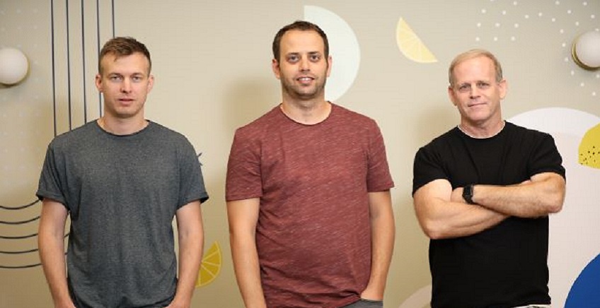
Photo above:Deci’s founders (from left to right): Jonathan Elial- COO, Yonatan Giefman- CEO and Ran El Yaniv- Chief scientist. Credit: Deci
Deci, the deep learning company harnessing Artificial Intelligence (AI) to build AI, announced a new set of image classification models, dubbed DeciNets, for Intel Cascade Lake CPUs. According to Deci, its proprietary Automated Neural Architecture Construction (AutoNAC) technology automatically generated the new image classification models that significantly improve all published models and deliver more than 2x improvement in runtime, coupled with improved accuracy, as compared to the most powerful models publicly available such as EfficientNets, developed by Google.
While GPUs have traditionally been the hardware of choice for running convolutional neural networks (CNNs), CPUs, already more commonly utilized for various computing tasks, would serve as a much cheaper alternative. Although it is possible to run deep learning inference on CPUs, generally they are significantly less powerful than GPUs. Consequently, deep learning models typically perform 3-10X slower on a CPU than on a GPU.
As explained by Deci, its DeciNets closes the gap significantly between GPU and CPU performance for CNNs. With DeciNets, tasks that previously could not be carried out on a CPU because they were too resource intensive are now possible. Additionally, these tasks will see a marked performance improvement: by leveraging DeciNets, the gap between a model’s inference performance on a GPU versus a CPU is cut in half, without sacrificing the model’s accuracy.
“As deep learning practitioners, our goal is not only to find the most accurate models, but to uncover the most resource-efficient models which work seamlessly in production – this combination of effectiveness and accuracy constitutes the ‘holy grail’ of deep learning,” said Yonatan Geifman, co-founder and CEO of Deci. “AutoNAC creates the best computer vision models to date, and now, the new class of DeciNets can be applied and effectively run AI applications on CPUs.”
All networks were compiled and quantized using OpenVino, with latency measured on AWS instance c5.4xlarge with Cascade Lake CPU (16 vCPUs, batch size = 1)
“There is a commercial, as well as academic desire, to tackle increasingly difficult AI challenges. The result is a rapid increase in the complexity and size of deep neural models that are capable of handling those challenges,” said Prof. Ran El-Yaniv, co-founder and Chief Scientist of Deci and Professor of Computer Science at the Technion – Israel Institute of Technology. The hardware industry is in a race to develop dedicated AI chips that will provide sufficient compute to run such models; however, with model complexity increasing at a staggering pace, we are approaching the limit of what hardware can support using current chip technology. Deci’s AutoNAC creates powerful models automatically, giving users superior accuracy and inference speed even on low-cost devices, including traditional CPUs.”
In March 2021, Deci and Intel announced a broad strategic collaboration to optimize deep learning inference on Intel Architecture (IA) CPUs. Prior to this, Deci and Intel worked together at MLPerf, where on several popular Intel CPUs, Deci’s AutoNAC technology accelerated the inference speed of the well-known ResNet50 neural network, reducing the submitted models’ latency by a factor of up to 11.8x and increasing throughput by up to 11x.
Deci enables deep learning to live up to its true potential by using AI to build better AI. With the company’s end-to-end deep learning development platform, AI developers can build, optimize, and deploy faster and more accurate models for any environment including cloud, edge, and mobile, allowing them to revolutionize industries with innovative products. The platform is powered by Deci’s proprietary automated Neural Architecture Construction technology (AutoNAC), which automatically generates and optimizes deep learning models’ architecture and allows teams to accelerate inference performance, enable new use cases on limited hardware, shorten development cycles and reduce computing costs. Founded by Yonatan Geifman, Jonathan Elial, and Professor Ran El-Yaniv, Deci’s team of deep learning engineers and scientists are dedicated to eliminating production-related bottlenecks across the AI lifecycle.
We use cookies to personalize content and ads, to provide social media features and to analyze our traffic. We also share anonymous information about your use of our site with our social media, advertising and analytics partners. View more
What personal data we collect and why we collect it
We collect anonymous data on visitors in this website for business purposes such as enhancing user experience, digital marketing and search engine optimization.
We collect personal data such as email address and names on various forms - all forms present in this website include consent checkboxes and clear reason for collecting the data: general inquiries on our products, newsletter subscription, professional inquiries job applications. All forms are designed in accordance with GDPR requirements.
Comments
When visitors leave comments on the site we collect the data shown in the comments form, and also the visitor’s IP address and browser user agent string to help spam detection.
An anonymized string created from your email address (also called a hash) may be provided to the Gravatar service to see if you are using it. The Gravatar service privacy policy is available here: https://automattic.com/privacy/. After approval of your comment, your profile picture is visible to the public in the context of your comment.
Media
If you upload images to the website, you should avoid uploading images with embedded location data (EXIF GPS) included. Visitors to the website can download and extract any location data from images on the website.
Contact forms and newsletter
We use Gravity Forms as our platform of choice for all forms present in this website. Forms present in this website have been modified to fit GDPR requirements.
Unless specifically specified and approved by visitor, we do not use the collected data for marketing purposes.
We use Mailchimp to collect email addresses and send periodical marketing materials to our customers.
Handling and management of all email addresses and mailing operations is conducted under GDPR terms and guidelines provided by Mailchimp.
All subscribers are able to change their subscriptions preferences or unsubscribe at any given time.
Techtime has accepted the Data Processing Addendum agreement provided by Mailchimp for all its Mailchimp accounts.
All our lead collection forms have been altered in accordance with GDPR requirements and now include unchecked checkboxes in order to accept the explicit consent of the user prior to form submission.
Cookies
If you leave a comment on our site you may opt-in to saving your name, email address and website in cookies. These are for your convenience so that you do not have to fill in your details again when you leave another comment. These cookies will last for one year.
If you have an account and you log in to this site, we will set a temporary cookie to determine if your browser accepts cookies. This cookie contains no personal data and is discarded when you close your browser.
When you log in, we will also set up several cookies to save your login information and your screen display choices. Login cookies last for two days, and screen options cookies last for a year. If you select "Remember Me", your login will persist for two weeks. If you log out of your account, the login cookies will be removed.
If you edit or publish an article, an additional cookie will be saved in your browser. This cookie includes no personal data and simply indicates the post ID of the article you just edited. It expires after 1 day.
Embedded content from other websites
Articles on this site may include embedded content (e.g. videos, images, articles, etc.). Embedded content from other websites behaves in the exact same way as if the visitor has visited the other website.
These websites may collect data about you, use cookies, embed additional third-party tracking, and monitor your interaction with that embedded content, including tracing your interaction with the embedded content if you have an account and are logged in to that website.
Analytics
We use Google Analytics regularly for monitoring user behavior and traffic sources and utilize the gathered information for enhancing user experience and for business purposes.
The use of Google Analytics in done according to GDPR terms and guidelines provided by Google.
Legal Entity: Techtime.
Primary Contact (a.k.a. "Notification Email Address"): roni@techtime.co.il - this email is designated for receiving notices under the Google Ads Data Processing Terms.
Who we share your data with
We use various cloud platforms and third party providers for the purpose of operating this website.
We do not share or sell your data for any commercial purpose other than specified above.
We use the following processors for the operating this website and executing related digital marketing campaigns:
WP Engine - Hosting Provider
Cloudflare - Cloud based security and web performance processor.
Google Cloud Platform - data centers provider for WP Engine
Sucuri - Website security provider
Mailchimp - Newsletter service provider
Google Analytics, Adwords, Webmasters
Facebook - We use Facebook for advertising and place tracking code on our website for enhancing digital marketing campaigns (i.e - Facebook Pixel).
Planwize Ltd - Digital Marketing Agency.
How long we retain your data
If you leave a comment, the comment and its metadata are retained indefinitely. This is so we can recognize and approve any follow-up comments automatically instead of holding them in a moderation queue.
For users that register on our website (if any), we also store the personal information they provide in their user profile. All users can see, edit, or delete their personal information at any time (except they cannot change their username). Website administrators can also see and edit that information.
What rights you have over your data
If you have an account on this site, or have left comments, you can request to receive an exported file of the personal data we hold about you, including any data you have provided to us. You can also request that we anonymize or erase any personal data we hold about you. This does not include any data we are obliged to keep for administrative, legal, or security purposes.
Request for Receiving Data Associated with One’s Email Address
Users may request to receive access to all related information submitted to this website for their review.
In accordance with GDPR compliance, user may further request the anonymization of such data.
In order to request access for all data associated with a given email address, users may submit the request here. Users then receive an email with a link to a page with all related information.
The link is valid for 24 hours. Users may submit additional request for the same email address once in every 24 hours.
A request for anonymization should be sent separately: User may select the data he or she wishes the site owner to anonymize so it cannot be linked to his or her email address any longer. An email confirmation will be sent once linked data has been successfully anonymized.
Where we send your data
Visitor comments may be checked through an automated spam detection service. All our processors and third party providers comply with GDPR requirements and apply privacy by design and necessary measure to ensure that personal data is being processed and handled in accordance with requirements. The list of our third party service providers and processors is listed above.
Contact information
For all privacy-specific concerns inquiries, you may contact us at mail@mail.com
How we protect your data
We use rigorous practices in order to protect our website and data collected, as well as world class cloud and hosting providers.
Communication between visitor and the server is encrypted using SSL.
The site is protected with web application firewall and is undergoing daily security scans, regular software updates by a dedicated team in order to minimize the risk of data breach.
What data breach procedures we have in place
Once a data breach is detected, our providers execute a dedicated standard operational procedure in order to assess the scope and potential damage, provide immediate remedy, patch any potential security holes and notify users who may be affected by the breach.
We may contact affected users with one or more form of communication within 72 hours and provide the needed information as to the scope of the data breach and actions taken.
What third parties we receive data from
We do not receive data from third parties for our marketing campaigns.
What automated decision making and/or profiling we do with user data
We may apply remarketing/retargeting methods while conducting online advertising using Google Facebook and the likes.
The above is conducted by applying various tracking codes into our website in order to track and retarget users based on
By visiting and using this website you are hereby provide your consent for the use of the above means and methods.