Exclusive: New E-beam microscope has brought Applied Materials down to the single Nanometer
8 August, 2016
A new type of electronic beam microscope and a revolutionary inspection methodology, both developed in Israel, could cut the inspection times of Nanometric sturctures from 50 years - to minutes

A new type of electronic beam microscope and a revolutionary inspection methodology, both developed in Israel, could cut the inspection times of Nanometric sturctures from 50 years – to minutes

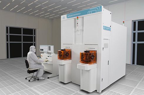
Applied Materials has recently launched its PROVision system, which was developed by the Israeli division (PDC) of the global corporation, located in Rehovot, near Tel-aviv. The system is designed for the inspection of silicon wafers during the manufacturing process. It supplies up to 350,000 images per wafer in a resolution of up to 1.5 nanometer. The new system has already been supplied to more than a dozen customers including some repeat orders from a leading foundry and a major memory manufacturer.
During an interview with Techtime, the chief technology officer for electronic based inspection products at Applied Materials Israel, Ido Holzman, revealed the revolutionary concept behind the new system.
Holzman: “Our system, i believe, is the highest resolution inspection machine in the industry. We have successfully developed of a high powered electronic microscope that brings to the surface a fourth fold amount of electrons on a given area, than we had before. It gives these machines the ability to inspect 10, 7 and 5 nano meter production lines. In the future we may be able to inspect even 3 nano meter processes.”
Combining Meteorology with Defect Inspection
Beside powerful e-beam, the Israeli team also revolutionized the way wafer inspection is performed at the manufacturing plant. “Two main inspection procedures are used by the industry: Metrology systems that preform measurements for process control and are located in several stations along the production line, and scanning inspection systems to detect defects within the chips. The product of the scan inspection system is a file reporting the amount of defects detected, as well as their characteristics.
“The majority of the inspection systems are optical. They are fast but effective in resolutions higher than approximately 100 nano meter. We overcome this restriction by analyzing interference effects characteristic to periodic structures. This enables us to detect defects of up to 10 nano meter. The problem is, that optics is blind to smaller defects.”
50 year to inspect a single wafer
“The problem is that new generations of semiconductor chips needs much higher resolutions. To inspect a 5 nanometer structure, for example, one needs an inspection resolution of at least 1 nano meter. Electronic microscope can give us the desired resolution, but a scan like this will extremely slow. When a wafer is scanned at a 1 nano meter resolution, an image of 10^16 pixels is generated. According to our calculations, it will take at least 50 years to process a single image like this!
“Our solution to this problem is based on the detection of relatively large random defects using optic methods, and later to the focus a high powered electronic microscope of specific sectors which are likely to be damaged. In order to do so, we analyze the design file itself, determine which areas are potentially sensitive to damages and likely to develop defects. These target areas are then inspected by the electronic microscope. We actually combined Metrology with Inspection.
“The idea is that in wafer areas where you find irregularities with Metrology tools, you are also likely to find chip level defects. The Metrology systems produce a map of measurements, a kind of personal signature for each phase in manufacturing process. Because we know the defect signature of various production machines used by the industry, we can perform a focused inspection of suspected areas.”
How do you cope with energy problems? Don’t the electrons affect the inspected transistors?
“Our technology is suitable for the inspection of specific layers during the complete inspection process, because the electrons can in fact affect the material. But we can choose the energy levels which the inspection system uses. The system enables us to work in various levels between 150 and 150,000 Volts. The user can choose the energy level according to his specific needs.”
Posted in: Featured Stories , News , Semiconductors , Technology


