Improved DAC Phase Noise Measurements Enable Ultra Low Phase Noise DDS Applications
7 June, 2018
Phase noise is a concern for all radio systems, but radar in particular can require phase noise performance at frequency offsets much closer to the carrier than a communication system

By: Peter Delos and Jarret Liner, Analog Devices
In radar applications, phase noise is a critical performance metric for systems requiring high clutter attenuation. Phase noise is a concern for all radio systems, but radar in particular can require phase noise performance at frequency offsets much closer to the carrier than a communication system.
System designers in these high performance systems will choose ultra low phase noise oscillators and the objective of the signal chains, from a noise perspective, is to add minimal degradation to the oscillator phase noise profile. This requires residual or additive phase noise measurements of the varied components in the signal chain.
Recent product releases of high speed digital-to-analog converters (DACs) are extremely attractive for both waveform generation and frequency creation for any LOs needed in frequency conversion stages. The radar objectives, however, challenge the DAC phase noise performance.
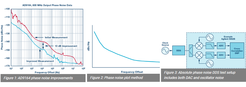
In this article, we show measured improvements of over 10 dB at 10 kHz offsets using the AD9164 DAC. Figure 1 illustrates the improvement and we will discuss how the results were achieved through a combination of both power supply regulator selection and test setup improvements.
Phase Noise Definition
Phase noise is a measure of the deviation in the zero crossing of a periodic signal. Consider a cosine wave with phase fluctuations:

Phase noise is determined from the power spectral density of the phase variations:

In linear terms, the single sided phase noise is defined as:

Phase noise is normally expressed in units of dBc/Hz from 10log(L(f)). Phase noise data is then plotted at offset frequencies relative to the RF carrier.
An important further definition of phase noise is absolute phase noise vs. residual phase noise. Absolute phase noise is the total phase noise measured in the system. Residual phase noise is the additive phase noise of the device under test. This distinction becomes critical in the test setups and in the process of determining component level phase noise contributions in a system.
DAC/DDS Phase Noise Measurement Methods
The figures in this section illustrate DDS phase noise test setups. For DAC phase noise measurements, it is assumed the DAC is used as part of a direct digital synthesizer (DDS) subsystem. A DDS is implemented with a digital sinewave pattern to a DAC that could be in a monolithic IC or an FPGA or ASIC communicating to a DAC. In modern DDS design, the digital phase errors can be made much less than the DAC errors, and DDS phase noise measurements are typically limited by the DAC performance.
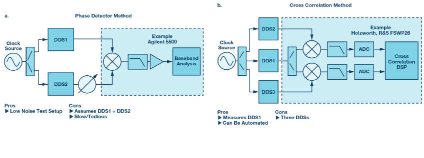
 The simplest and most common test setup is shown in Figure 3. A clock source is used for the DDS and the DDS output is fed to a cross correlation type phase noise analyzer. This is easy to implement since only a single DDS is required. However, with this test setup, there is no method to extract the oscillator contribution to show only the DDS phase noise.
Figure 4a shows the phase detector method. In this case, two DACs are used and the oscillator contribution subtracts from both DUTs in the downconversion to dc.
Figure 4 shows two common methods to remove the oscillator phase noise from the measurement, providing a residual noise measurement. The drawback of the measurements is that additional DACs are required in the test setup. However, the benefit is a much better indicator of the DAC phase noise contribution that can be applied in system-level analysis budgets.
Figure 4b shows a method using cross correlation phase noise analysis. In this case, DDS2 and DDS3 are used to translate the clock contribution to the LO ports of the measurement, their contribution is removed in the cross correlation algorithms, and the DDS1 residual phase noise is obtained in the measurement.
Power Supply Noise Contributions
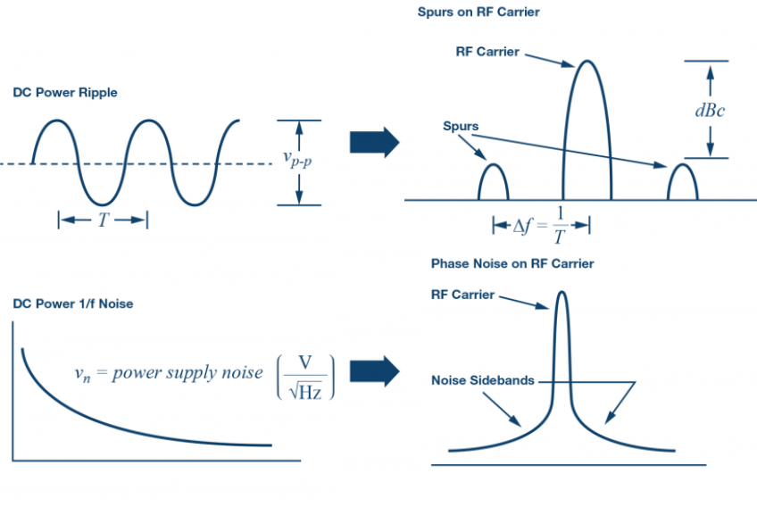
In low noise analog and RF design, power supply noise is a well-known factor to consider. Power supply ripple that is periodic modulates onto the RF carrier and creates spurs on the RF carrier at frequency offsets equal to the ripple frequency. Regulator 1/f noise modulates onto the RF carrier also and contributes to the phase noise profile. Figure 5 illustrates the principles.
Measured Results
During investigation of the true DAC phase noise performance, both the test setups and the regulator noise performance were considered.
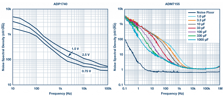
The initial DAC evaluation board included the ADP7140 regulator for the analog and clock voltages. Noise spectral densities were compared with recently released ultra low noise regulators and the ADM7155 was chosen. Figure 6 illustrates the comparison of the noise densities as shown in the product data sheets. The power supply modification was merely to use the ADM7155 for both the AD9164 clock (data sheet pins VDD12_CLK) and the analog voltage (data sheet pins VDD12A).
Next, test setup options were considered for residual phase noise measurements. The cross correlation method was chosen with the Rohde and Schwarz FSWP primarily out of availability and convenience. The test setup used is shown in Figure 7.
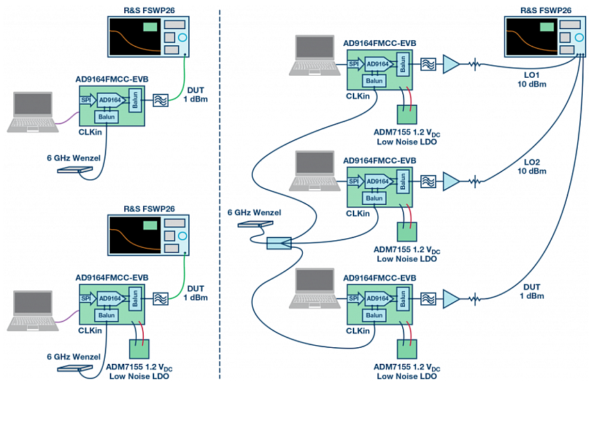
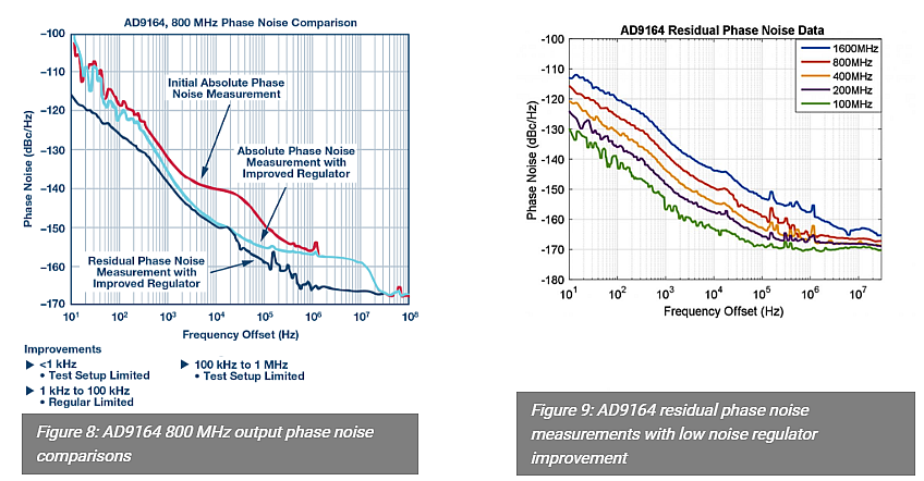
Figure 8 is a measurement of three cases. The initial evaluation board measurement taken with an absolute phase noise approach is shown as the red curve. The light blue curve is also an absolute measurement, but with the regulator improvement. The dark blue curve is a residual phase noise measurement that also includes the regulator improvement.
The measurement indicates three general regions of limitations in the initial measurement that were not obvious in the beginning of the investigation. Frequencies below 1 kHz were limited by the close in noise of the clock source. Frequencies from 1 kHz to 100 kHz were limited by the regulator selection. Frequencies above 100 kHz were limited by the clock source. The sharp drop off above 10 MHz is the clock source contribution, as the clock used was a multiplied crystal oscillator to create 6 GHz and the roll-off is from the RF filters used in the multiplication stages.
Residual phase noise measurements with the regulator improvement were taken at additional DAC frequencies and several are summarized in Figure 9. The modifications were duplicated on several evaluation boards and all cases showed the same improved results.
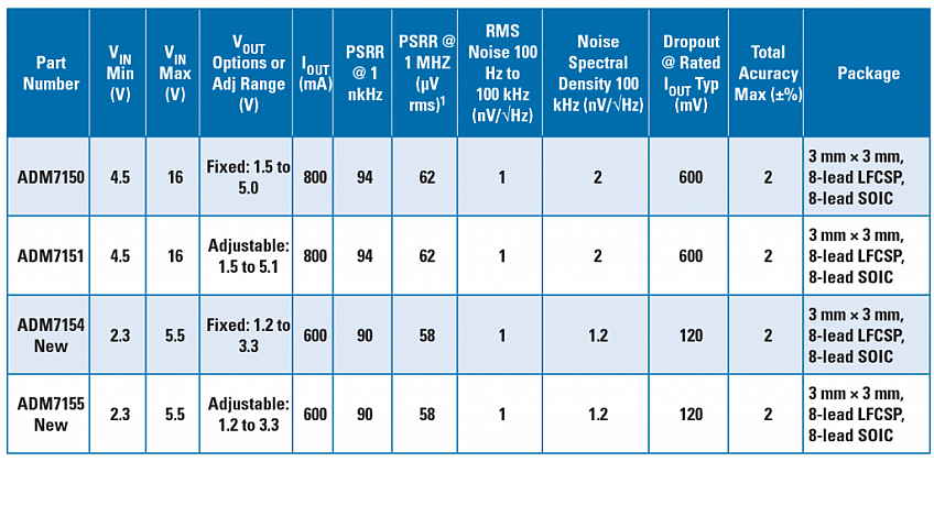
 The family of ultra low noise regulators with similar noise density is shown in Table 1. As demonstrated, the impact on the DAC phase noise is significant and these are also recommended for consideration for any areas of the RF system requiring optimum phase noise performance.
Summary
A phase noise review was provided for the fundamental definition, absolute vs. residual phase noise, DAC phase noise measurement test setups, and regulator noise contributions.
DAC phase noise improvements were demonstrated for including both residual phase noise test methods and optimum regulator selection. The end result is the AD9164 now is an enabler for ultra low phase noise, DDS-based applications when the analog voltages and clock voltages are powered from the Analog Devices family of low noise regulators.
References:
- Bergeron, Jarrah, “Analyzing and Managing the Impact of Supply Noise and Clock Jitter on High Speed DAC Phase Noise,” Analog Dialogue, Vol. 51, 2017.
- Calosso, Claudio E., Yannick Gruson, and Enrico Rubiola, “Phase Noise and Amplitude Noise in DDS,” IEEE Frequency Control Symposium, 2012.
- Jayamohan, Umesh, “Powering GSPS or RF Sampling ADCs; Switcher vs LDO,” Analog Dialogue, Vol. 50, 2016.
- “Product Note 11729B-1, Phase Noise Characterization of Microwave Oscillators: Phase Detector Method,” Agilent, May, 2007.
- Reeder, Rob, “Designing Power Supplies for High Speed ADC,” Analog Devices, Inc., 2012
- Walls, Warren F. “Cross Correlation Phase Noise Measurements,” IEEE Frequency Control Symposium, 1992.
Authors
Peter Delos [peter.delos@analog.com] is a technical lead at Analog Devices, Inc., in the Aerospace and Defense Group. Jarrett Liner [ jarret.liner@analog.com] is an RF systems application engineer with Analog Devices, Inc., in the Aerospace and Defense Group in Greensboro, NC.


