Photonics goes into the Chip
9 December, 2015
Joris Van Campenhout of imec: “If we want to make silicon photonics technology cost-effective, we have to optimize the packaging.”
“If we want to make silicon photonics technology cost-effective, we have to optimize the packaging.”
By: Joris Van Campenhout, imec *
 Optical data transmission is a key answer to the ever growing data traffic. Today, data centers make use of hundreds of thousands optical links that interconnect the server racks at network rates up to 40Gb/s. In the coming years, the technology needs to be even more performant: 100Gb/s in 2016, 400Gb/s by 2019, even Terabit/s on the longer term.
On top of that, data center operators put forward a cost target of 1$ per Gb/s.
Optical interconnects will also be deployed at shorter distances – within the server rack, on the board or even on chip. And this is even more challenging. What we need is a scalable technology that consumes little power (less than a pico Joule per bit), and can be fabricated in large volumes at low price.
At imec, we use silicon photonics technology to make optical transceivers. In 2015, we showed that our technology is scalable in terms of performance: we demonstrated several building blocks (silicon ring modulator, germanium-based electro-absorption modulator, (de-)multiplexing filter, germanium-on-silicon photodector) achieving date rates of 50Gb/s.
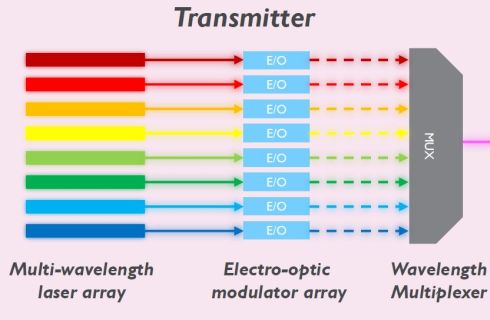
By multiplexing the signals on eight different wavelengths, we can make optical modules of 400Gb/s. Also, the technology offers a route towards Terabit/s, for example by adopting more advanced modulation schemes. And by implementing the silicon photonics platform on 300mm wafers, we will be able to enhance the optical performance and make the platform compatible with the latest 3D integration technologies.
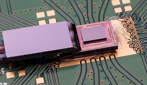
But if we want to reach our cost target, additional efforts are needed. In particular, the assembly and packaging of the technology – in particular, the interconnection and alignment of the different building blocks – raise the cost. Our technology has an important advantage with respect to discrete photonics: by integrating the modulators, the filters and the detector on a single chip, these building blocks are automatically aligned.
In 2015, we demonstrated this integration of building blocks, and showed that our solution works at the system level, and at low voltages. However, the alignment of the optical fiber is still a challenge to overcome. Today, we use an active alignment: we send light through the fiber, couple the fiber and the chip, and once the coupling is optimal, we glue them together.
![]()
Such a solution is very slow and expensive. In order to make the modules in larger volumes, we need passive alignment. And this can only be realized with more tolerant interfaces between fiber and chip. Today, the alignment accuracy as required by the interfaces is still too large (1 micron or smaller).
The lasers that generate the carriers for the data signals face the same problem. The future is to passively aligned, hybridly integrated lasers. Or, on a longer term, monolithically integrated lasers grown directly on the substrates. This way, we do not longer need a laser-to-wafer assembly. In 2015, we took an important step forward. In collaboration with Ghent University, we demonstrated the first arrays of indium phosphide lasers monolithically grown on 300mm substrates.
* Joris Van Campenhout – program director optical I/O, imec
Joris Van Campenhout is program director of the Optical I/O industry-affiliation program at imec (Belgium), which targets the development of a scalable and industrially viable optical-interconnect technology based on Si photonics. Prior to joining imec, he was a post-doctoral researcher at IBM’s TJ Watson Research Center (USA), where he developed silicon electro-optic switches for chip-level reconfigurable optical networks. He obtained a PhD degree in Electrical Engineering from Ghent University (Belgium) in 2007, for his work on hybrid integration of electrically driven III-V microdisk lasers on Si-photonic waveguide circuits.
Posted in: ElectroOptics , Featured Stories , News , Semiconductors

