What’s Driving the Demand for HBM3?
24 October, 2021
Through vertical stacking of memory chips and by connecting to the host SoC via 2.5D interposer technology, High Bandwidth Memory (HBM) promises to prevent memory bandwidth from turning into a bottleneck

Sponsored by Synopsys. By Graham Allan, Sr. Staff Product Marketing Manager, Synopsys Solutions Group, and Vikas Gautam, VP of Engineering, Synopsys Verification Group
Applications with data-intensive workloads can’t afford a slowdown. To prevent memory bandwidth from turning into a bottleneck, higher speeds to move data between the system’s processor and its memory are in demand. That’s where high-bandwidth memory (HBM) interfaces come into play. Bandwidth is the result of a simple equation: the number of bits times the data rate per bit. For example, a DDR5 interface with 64 data bits operating at 4800 Mbps would have a total bandwidth of 64 x 4800E+06 = 307.2 Gbps = 38.4 GBps.
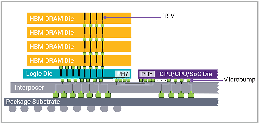
To achieve higher data rates, you can either increase the data rate or the width of the bus. DDR5, LPDDR5, and GDDR all take the approach of ramping up the data rate, which causes signal integrity issues as the time for each bit to transfer across the bus shrinks. HBM, however, uses the “go wider” approach, employing a data bus that is 1024 bits wide. In order to accommodate such a wide bus, HBM-based designs employ a 2.5D interposer to connect the host to the DRAMs, which is effectively a miniature PCB that goes inside the package, as shown in the image below.

HBM provides a high-speed memory interface for 3D stacked synchronous dynamic random-access memory (SDRAM). Soon after commercial HBM memory chips were made available, in early 2013, JEDEC released HBM as an industry standard later that year. The latest step in the evolution is HBM3, which is currently under discussion by JEDEC and could be released as a standard as early as late this year.
In this article, which was originally published on the “From Silicon to Software” blog, we’ll take a closer look at what’s driving the demand for HBM3 and how you can continue to feed our world’s growing appetite for bandwidth.
Architected for High Bandwidth and Low Power
IDC predicts that by 2025, worldwide data will grow to 175 zettabytes, representing a 61% compounded annual growth rate from 33 zettabytes in 2018. Three key locations in this datasphere are traditional and cloud-based data centers, followed by the edge (such as cell towers and branch offices), followed by endpoints (such as IoT devices and smartphones). Through vertical stacking of memory chips and by connecting to the host SoC via 2.5D interposer technology, HBM technology shortens the length in which data must travel, supporting smaller form factors. Its 1024-bit memory bus is significantly wider than that of other DRAM types.
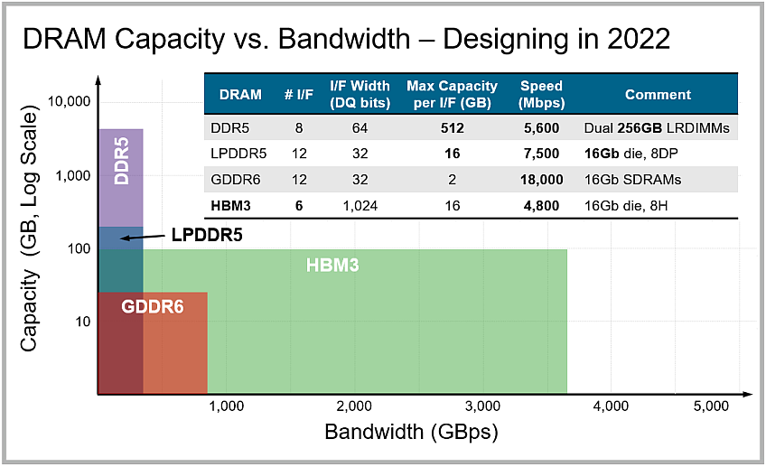
With their high bandwidth and low power consumption owing to shorter, unterminated signals, these interfaces are well-suited for graphics cards, as well as server, high-performance computing (HPC), networking, and high-end AI and machine-learning applications. (The hyperscale data centers that are garnering much buzz these days are driven more by the need for expanding capacity, so their memory type of choice is DDR5.) The graph below highlights the differences in DRAM capacity and bandwidth among different memory types.

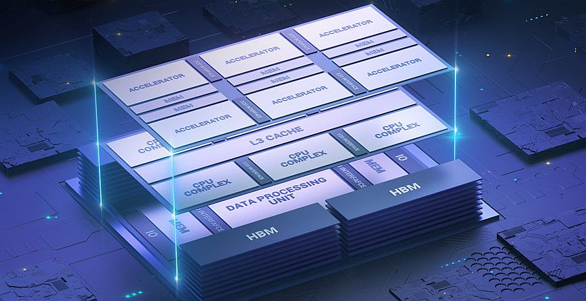
HBM brings 3D content into 2.5D designs, which typically consist of a GPU or host SoC and multiple HBM “stacks” assembled side-by-side on an interposer in a single package. Such designs have been an AI workhorse for almost a decade now and are finding their way into market segments such as 5G infrastructure, data centers, and large networking systems. The HBM2E standard enables 8- and 16-GB capacities, with 3.6-Gbps transfer rates and 461-GBps total bandwidth.
The stacked architecture of HBM3 will drive 3DICs for data-intensive applications, providing a way to alleviate the challenges of reticle, die size, and interposer limits. Speculation on what HBM3 will deliver yields these specs:
-
- Bandwidth up to 819 GBps
- Capacity up to 64 GB per stack (as specified by the JEDEC standard, though expect less for real products)
- 6400-Gbps transfer rates
- More dies per stack and more than 2x the density per die with a similar power budget
- The lowest power efficiency of any off-chip DRAM owing to short, unterminated channels.
Although HBM3 has not yet been standardized, some in the industry have already announced designs featuring the super-fast memory. For example, SK hynix has discussed its HBM3 technology that’s in development, noting that it “will be capable of processing more than 665GB of data per second at 5.2 Gbps in I/O speed.”
Unique HBM Design Considerations
Based on its stacked architecture, designing with HBM comes with some unique challenges, the interposer being one of the most notable. An electrical signal conduit, the silicon interposer connects the stacked SDRAM to the processor. There are many design rules around the interposer, which must be custom developed for each chip. The component also adds to the expense of the design.
Logic and DRAM dies are fabricated separately. As part of the HBM flow, through-silicon vias (TSVs), providing the vertical interconnects for the interposers, are formed in each DRAM die, and their uniformity is critical. Microbumps formed on top of the die to provide electrical connections between the different dies create additional challenges related to these fine-pitch structures.
Another HBM design consideration is the limited number of SDRAMs to connect to. With SoCs becoming more complex, especially at advanced nodes, there may only be room for 4-6 HBM stacks as the interposer reaches reticle limits. Once such a chip is built, there’s no flexibility in changing its design down the road, so this should be accounted for at the start of the process. Heat dissipation, too, is an important challenge since DRAMs lose their storage bits faster to leakage at higher temperature. That can be addressed via lidless packaging technology that allows the heatsink to contact the silicon directly.
Solving Bandwidth Bottlenecks
With the runway to HBM3 shortening as we head to the end of 2021, it’s a good time to make sure that you have in place what you’ll need to keep feeding the hunger for bandwidth. Memory interface IP can help you achieve your memory throughput requirements with minimal power consumption and low latency, while reducing integration risks. Verification IP aligned to the latest protocols helps accelerate runtime, debug, and coverage closure for your designs.
As we continue our efforts to stay ahead of emerging standards, Synopsys has recently announced the industry’s first complete HBM3 IP solution, including controller, PHY, and verification IP for 2.5D multi-die package systems. Synopsys DesignWare® HBM3 Controller and PHY IP, built on silicon-proven HBM3E IP, tap into our interposer expertise to provide a low-risk solution supporting high memory bandwidth up to 921 GBps.
On the verification side, our offerings include our Verification IP with built-in coverage and verification plans, as well as off-the-shelf HBM3 memory models for Synopsys ZeBu® emulation and HAPS® prototyping systems. Additionally, Synopsys 3DIC Compiler multi-die design platform accelerates development of HBM3 system designs through fully integrated architectural exploration, implementation, and system-level analysis.
In a recent news release about our new HBM3 offerings, Cheol Kyu Park, vice president, HBM product champion, and head of DRAM product engineering at SK hynix, noted, “We will leverage our long-standing relationship with Synopsys to provide our mutual customers with fully-tested and interoperable HBM3 solutions that can maximize memory performance, capacity and throughput.”
Memory bandwidth doesn’t have to become a bottleneck. HBM continues evolving to provide a reliable way to quickly move data between a system’s processor and its memory. Once HBM3 becomes standardized, the protocol promises to bring even faster speeds and lower power consumption to our most compute-intense applications.


