University Program Nurtures Next Generation of Engineers
9 November, 2021
Close collaboration between businesses and universities can help nurture the next generation of engineers. Tel Aviv University and North Carolina State University provide striking example

By Patrick Haspel, Global Program Director, Academic Partnerships and University Programs, Synopsys
The COVID-19 pandemic has accelerated our digital migration, moving more of our activities online. Ajit Manocha, president and CEO of SEMI, has discussed how critical it will be for the industry to close the talent gap. Investing in science, technology, engineering, and math (STEM) education is one way to nurture the interests and skillsets that are needed to bring more engineers into the workforce.
Collaborative business/university relationships, where businesses provide resources that complement or augment educational programs, provide a nice bridge between the two worlds. One such example is the Synopsys Electronic Design University Program, which provides academic and research institutions with access to electronic design automation (EDA) software, technical support, curriculum, and more.
The university bundle consists of more than 200 tools for a nominal fee and licensing agreement in support of fundamental research and education efforts. In this article, which was originally published on the From Silicon to Software blog, I’ll highlight some key examples that illustrate the mutually beneficial outcomes that are resulting from close collaboration between the business and academic worlds.
VLSI Training Course at Tel Aviv University
Creating the next generation of chip design engineers needs to start at the university level. Consider a project involving a complex 5nm design, which would require a team for implementation, verification, software design, and more. Such an endeavor could involve more than 100 people who have the latest skills. However, it’s not always easy to find the right mix of engineers.
Israel, for example, is in a region of the world where the dearth of electronic design talent is extremely high. To help create a pipeline of engineers, Zvi Webb, a retired applications engineering director from Synopsys, is serving as VLSI lab manager at Tel Aviv University and is developing an introductory very large-scale integration (VLSI) course based on the latest chip design tools. Students there, Webb noted, hadn’t been exposed to a digital design workflow and tool chain. Instead, they were building their designs manually.
Webb’s course will be offered in the spring of 2022 and will cover topics such as Verilog, logic synthesis, static timing analysis, and placement and routing, providing students with real-world expertise that can help open doors once they’re ready for the workforce. The training outline was derived from material prepared by Professor Adam Teman from Bar Ilan University. “The new course will bring student engineers more knowledge – they will gain an understanding of what VLSI means, what the steps are, how to perform checks,” Webb said.
NC State University Creates PDK for Physical Verification at 3nm
What constitutes an effective 3nm node? According to research conducted by the Electrical & Computer Engineering Department at North Carolina State University, which based its examinations on several IMEC papers, the 3nm node is marked by a gate length of approximately 15nm, cell track height of 5.5T, and contacted poly pitch of 42nm. Scaling has been enabled by design technology co-optimization to achieve the desired benefits; however, as Moore’s Law slows down, it’s now also important to look at system technology co-optimization, examining ways to reengineer the power grid and utilize new device structures (such as gate all-around FETs).
Dr. Rhett Davis, a professor at the university’s Electrical & Computer Engineering Department, has teamed up with graduate students, other faculty, and the Synopsys University Program to create an open-source 3nm process design kit (PDK) for education and industry research. Specifically, the team wanted to explore the impact of new structures like gate all-around FETs and scaling boosters like buried power rails and 5.5T height metal pitch.
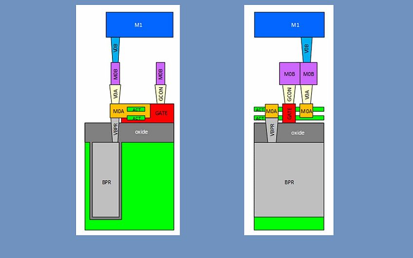
“What we found when making this kit is that transistors aren’t really shrinking anymore. Instead, they’re getting taller. That is, foundries are finding economical ways to stack them. Our kit compiles the best available public data into a set of rules that show us how to work with this new technology,” explained Davis.
To create the resulting FreePDK3, the team used Synopsys IC Validator for physical verification, Synopsys Custom Compiler for layout and schematic entry, Synopsys StarRC for parasitic extraction, and HSPICE® technology for circuit simulation. The FreePDK3 is published on the GitHub repository.
Engaging the Next Generation of Engineers
These examples illustrate the work that academia is engaging in with the business world. Through our Electronic Design University Program, Synopsys provides full-semester coursework for undergraduate and graduate programs in IC design and EDA development; teaching resources such as libraries and PDKs, and technical support and training. In addition, Synopsys also offers academic programs in the areas of optical design and static analysis software.
The Synopsys Foundation is committed to advancing STEM education opportunities that contribute to the growth and development of our future technology leaders. Through close collaboration, businesses and universities can help nurture the next generation of engineers for semiconductor and electronics industries that are continuing to embark on new innovations that are fueling our smart, connected world.
Posted in: blogs , News , Semiconductors
Posted in tags: semiconductors , synopsys


