Panther Lake: The Processor Developed in Israel Alongside Its Manufacturing Process
7 September, 2026
A new Intel documentary reveals how Panther Lake was developed alongside Intel 18A—and the design changes demanded by PowerVia and modular architecture
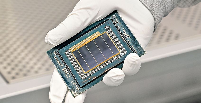
Panther Lake, Intel’s Core Ultra Series 3 processor family, is more than just a new generation of laptop processors. It is also the company’s first product to be manufactured at high volume using the Intel 18A process. As such, it represents a major test of Intel’s ability to return its manufacturing technology to the forefront of the semiconductor industry—and eventually offer it to external foundry customers as well.
In a new 90-minute documentary released by Intel, the program’s managers and engineers describe a development process that began in 2021 and involved thousands of employees around the world. While the film was produced by Intel and frames the project as a success story, it also provides a revealing look at the challenges of developing a processor and the manufacturing process on which it depends at essentially the same time.
Intel’s Israeli development center played a central role in the project. According to the documentary, the product definition process began in a room at the company’s Israeli R&D center, where teams tried to anticipate what the PC market would look like two or three years into the future. The compute tile and CPU cores were developed in Israel, while the graphics technology was developed by teams in Folsom and India. Other components came from additional Intel sites worldwide.
The Israeli executives and engineers featured in the documentary include Zohar Tzaba, vice president and Panther Lake program manager; Yaron Ananki, vice president and head of the Client Development Group; Erik Gihon, senior principal engineer for SoC architecture; Hagai Burstein, product development engineering manager; and Liel Elgarably, client platform integration engineer.
Lunar Lake Efficiency, Arrow Lake Performance
The architectural starting point for Panther Lake was an effort to combine the strengths of Intel’s two preceding processor families.
“Panther Lake is a combination of Lunar Lake and Arrow Lake. We took the best of both worlds and brought them together,” Erik Gihon explains in the film.
From Lunar Lake, Intel carried over power efficiency, battery life and the NPU. From Arrow Lake, it drew performance, scalability and a higher core count. In its largest configuration, Panther Lake features up to 16 CPU cores, compared with eight in Lunar Lake, along with integrated graphics containing as many as 12 Xe cores. Its new performance cores are called Cougar Cove, while the efficiency cores are based on the Darkmont architecture. Both were adapted for the Intel 18A process.
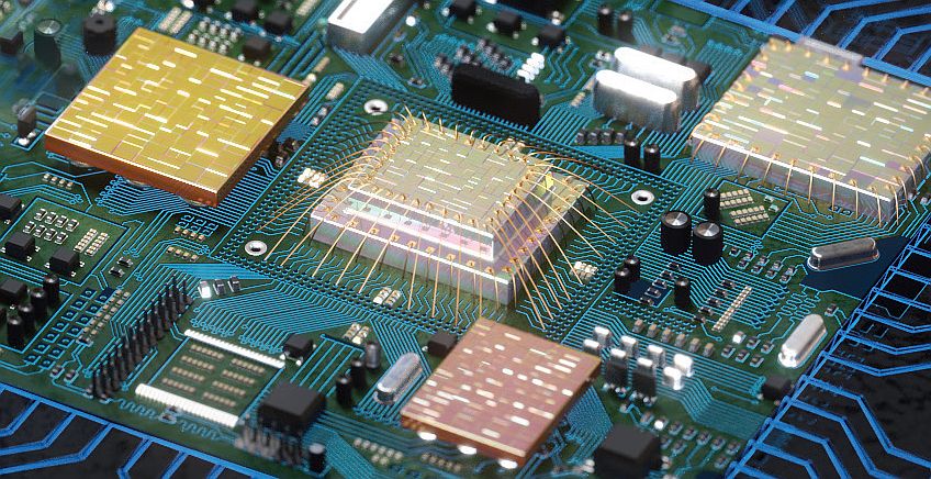
To address a broad range of PC designs, Intel moved from a monolithic architecture to a modular one. The family includes CPU, graphics and I/O tiles of varying sizes that can be combined in three main configurations. An eight-core version is aimed primarily at business laptops. A 16-core configuration with a larger I/O tile adds eight PCIe 5.0 lanes and is designed for PCs equipped with discrete graphics. The flagship version combines the larger processor with integrated graphics featuring 12 Xe cores.
A Manufacturing Process Still in Motion
The project’s unusual challenge stemmed from Panther Lake’s role as the “lead customer” for Intel Foundry’s 18A process. Unlike a product developed on a mature manufacturing node, Panther Lake was designed using evolving versions of the process design kit and frequently updated transistor-performance models.
The product teams had to anticipate how the manufacturing process would behave once it reached maturity and continually adjust the design accordingly.
Intel 18A introduces two major technological changes: RibbonFET, Intel’s gate-all-around transistor architecture, and PowerVia, a backside power-delivery system. In the documentary, Bill Grimm, product engineering manager in Intel Foundry’s Technology Development organization, describes 18A as “a revolutionary process, rather than simply an incremental improvement over the previous generation.”
PowerVia brings power connections closer to the transistors instead of routing them through 14 or 15 metal layers on the front side of the chip. The result is lower resistance, reduced area requirements and potential improvements in both performance and energy efficiency.
The change, however, also forced Intel’s engineers to redesign some of the signal-routing infrastructure. The front-side power-delivery network had previously provided shielding between sensitive signals. Once it was moved to the back of the chip, some metal lines had to be widened and spaced farther apart to prevent interference and preserve clock-signal integrity.
Making Progress With Imperfect Chips
Before the first silicon arrived, Intel tested the design, firmware and software using simulations, emulators and FPGA-based systems. It then began a gradual engineering-sample process. The first ES0 units initially operated at low frequencies. Performance improved through the ES1 and ES2 generations, eventually leading to the B0 revision, which was selected as the production candidate.
Because yields on the new manufacturing process were still limited, Intel developed a method for making use of units that were not fully functional. If only one section of a chip was defective, the unit could be assigned to a validation team that did not require that particular component. This allowed Intel to extract value from nearly every unit coming out of the fab and continue testing despite the limited supply of fully functional samples.
The modular architecture added another layer of complexity. Each processor combines CPU, graphics and I/O tiles produced on different wafers. It was therefore not enough to sort and test each tile separately; Intel also had to match the tiles in combinations that would produce a functioning processor at the required performance tier.
The Bet on B0
One of the project’s most consequential decisions came roughly six months before product qualification. Intel needed to begin building commercial inventory so that hundreds of thousands—and eventually millions—of units would be available at launch. At that point, however, the company still did not know with certainty whether the B0 revision was free of defects that might require another silicon stepping.
The decision was based on the progress of validation, the number of units tested, the status of known defects, yield forecasts and feedback from PC manufacturers. Program executives say it also involved an element of engineering judgment, drawing on the experience of the architects, developers and validation teams.
The gamble paid off: B0 became the production revision of Panther Lake.
At the same time, Intel was working with PC manufacturers on approximately 200 different system designs.
“If all 200 systems had been powered on for the first time at once, our validation and customer engineering teams would have been completely overwhelmed,” says Liel Elgarably.
Intel initially selected a small group of systems and brought them up and validated them together with the manufacturers. Only after resolving the first round of issues did it expand the process to the remaining designs.
The company also dramatically shortened the product-qualification stage. While qualifying the various Alder Lake packages took more than a quarter, Intel had to qualify the entire Panther Lake family within a single month. Findings from the first product were shared daily with the teams responsible for the other configurations, helping them avoid repeating the same tests and encountering the same problems.
For Intel, Panther Lake is therefore more than a new processor. It is the company’s first attempt to turn RibbonFET and PowerVia from laboratory-developed technologies into the foundation of a product family manufactured in tens of millions of units.
The documentary, however, does not disclose yield figures, rejection rates or manufacturing costs. The project’s success will ultimately be measured not only by the fact that Panther Lake reached the market, but also by its real-world performance, the availability of PCs based on the processor, and Intel’s ability to attract external foundry customers to its 18A process.
Watch the full documentary:
Posted in: News