The Tiny-huge road to 3D Semiconductor
22 December, 2015
"The standard interconnections in the industry have a pitch of 40um, but we are working to enable pitches down to 10, 5, or even 3um"

“The standard interconnections in the industry have a pitch of 40um, but we are working to enable pitches down to 10, 5, or even 3um”
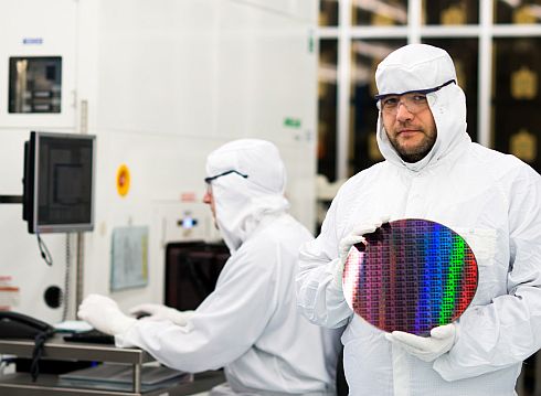
By: Eric Beyne, program director 3D Integration, imec
During the last 2 to 3 years, the technology of 3D integration has been developed into a technically and economically interesting road. In comparison to conventional planar 2D systems, we are now able to fabricate shorter and faster connections between circuits, and make these connections much denser, allowing a fine-grained partitioning of functions.
These abilities have made 3D integration one of the techniques that will allow the industry to keep on the path of Moore’s law. At the same time, it offers a practical way to scale systems with heterogeneous components.
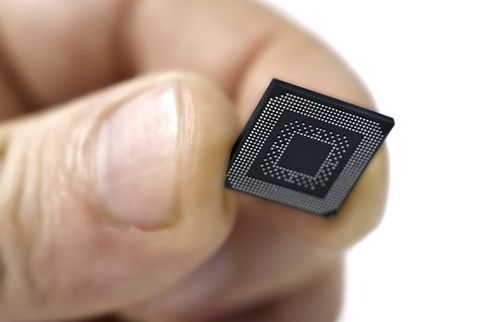
The first commercial 3D chips consist of conventional 2D chips stacked onto each other – 3D stacked ICs – was mostly in packages including DRAM memory chips. But in the coming years we expect to see stacked heterogeneous systems – 3D SoCs – hitting the market.
These are packages in which chips with varying functions and technologies are stacked very densely; think of image sensors with per-pixel readout and processing done by specialized chips connected on the level of the pixels.
The road to 3D-IC
Another step further we will see 3D-ICs, where instead of chips, layers of transistors are stacked. This concept is now being developed in the labs, and a first taste of what will become possible is given by 3D-NAND memory chips in which vertically stacked memory cells (sometimes more than 50!) share a common vertical transistor channel.
As one of the important technical challenges of 2016 and beyond, we work to improve the density of interconnections of 3D systems. This will allow to connect not only functional blocks, but also tiny sub-circuit units, such as pixel processors or memory cells.
These techniques are essential to fabricate the powerful chips needed for future supercomputers, multimedia applications or high-resolution image processing. But to enable these dense interconnections, the industry also needs more precise stacking and bonding techniques. Together with our partners in the 3D integration program, imec is assessing all design, technology, and processing options.
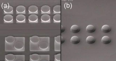
In 2015 we have made a substantial progress, both for die-to-wafer and wafer-to-wafer stacking, the two main roads to stack chips and connect them electrically. In die-to-wafer stacking, finished dies are bonded on top of a fully processed wafer. The standard interconnections in the industry have a pitch of 40um, but we are working to enable pitches down to 10, 5, or even 3um.
Imagine an interconnect of 1.8um
The challenge is to make these connections in a fast and accurate way with a high yield. We have developed new processes to interconnect micro-bumps through thermo-compression with the help of a new generation of ultra fast and accurate tools.
For wafer-to-wafer stacking, our ambition is to bond processed and thinned wafers with an accuracy down to 200nm. One of the challenge we have been working on has to do with the way the two extremely smooth wafer surfaces connect – they roll onto each other causing a slight deformation that is as large as the accuracy that we are aiming at. So we have to find ways to compensate for that.
To bond the wafers and connect them electrically, we work along two paths. One involves SiCN-bonding (silicon-carbon-nitride), and using ultra fine TSVs (through-silicon vias) for the connection. With this technique, we will thin down the upper wafer to 5um and scale the TSVs to a diameter of 1um.
For the second technique – hybrid bonding – we also use SiCN for the bonding, but we make the electrical contacts with small and ultra thin (5nm) copper facets. This allows us to reach a pitch down to 3.6um; in experiments we even reached interesting first results with a density of 1.8um.
Want to know more?
On these subjects, we published the following articles in our 2015 editions of imec magazine:
> Lightning-fast die to wafer stacking
> Exploring graphene on the interconnect test bench
> Polariscopy reveals TSV stress fields
> A novel approach for integrating ultralow-k dielectrics
> Imec compares yield of two major flavors of chip stacking
> When will we find 3D chips in our smartphones?
About the author
 Eric Beyne is program director of the advanced packaging and interconnect research at imec. This team performs R&D in the field of high-density interconnection and packaging techniques focused on “system-in-a-package” integration, 3D-interconnections, wafer-level packaging, RF front-end design and technology using integrated passives and RF-MEMS as well as research on packaging reliability including thermal and thermo-mechanical characterization.
Eric Beyne obtained his PhD in Applied Sciences in 1990 from the KU Leuven (Belgium). He has been with imec since 1986 and is president of the IMAPS-Benelux committee, member of the IMAPS-Europe Liaison committee, elected member of the board of governors of the IEEE-CPMT society and IEEE-CPMT Strategic Director for Region 8.
Posted in: Featured Stories , News , Semiconductors
