By: Andrea Vinci, Technical Marketing Manager at Tektronix/Keithley
The Semiconductor Industry is always searching for new special materials, dielectric solutions and new device geometries for scaling down the device size further and further. Lateral and vertical heterostructures of 2D materials for instance have led to new revolutionary tiny and low power electronics.
Researchers, Scientist and Engineers in the Industry all share a common headache when producing an accurate report of the electrical characteristics of such semiconductor devices, like special NANO-FETs, and even worse when they need to prove they can actually control these parameters in an easy and repeatable way.
It’s the typical problem of electrical characterisation in the low current range: the need to identify the attainable device performance under different conditions for low power/low leakage currents MOSFETs.
Measurements are critical since they identify those specific Figures of Merit (FoM) that confirm or not the effective behavior within specific applications. For instance, n-type FET require to evaluate ON and OFF drain currents at different values of source, drain and gate voltages. FoMs can vary across applications, but the way to obtain them is essentially common: something sources a precise and controlled level of voltage or current that varies in a certain way, while voltage and current measurements are also accurately taken to be correlated with each specific variable variation.
The problem is practically solved by using a certain number of Source Measure Units (SMUs), special instruments capable of sourcing current or voltage while measuring both current and voltage. But wherever a practical solution seems readily available, a lot of hidden “details” may cause failures and misleading results. Let’s explore them.
A critical question you should ask yourself
Often, engineers fall into the trap of forgetting to carefully look holistically into their test system. Or better, they clearly see their device, and they clearly see their instruments, but they miss to see what’s in between. For instance, I have seen multiple times users of oscilloscopes forgetting about the fact they were using probes to reach the specific test point to measure on their circuit board.
Those who reminded to consider the effect of the probe on signals, they anyway tended to forget about the probe leads effect on the measurement and problems related to signal coupling. “Come on, does it also really matter?”, they asked. Everything does. Unfortunately. And we need to take this into account.

For DC characterisation applications the risk is similar. Even if the physical probing on the device is essentially left to a complex and expensive probe station system, the SMUs that have to force the voltage and measure the current, they are connected to the probe card by means of cables. Should we consider cables as potentially affecting our measurements results? Regardless of the answer, what matters is that you always ask this question to yourself before proceeding, and more important, make sure that your answer is correct.
Precision measurements in CMOS manufacturing are a typical example where connectivity matters. Connectivity in fact means capacitances to be added to the test system. And since todays MOSFETs are characterised over a wider extended frequency range, any added capacitances effect must be carefully taken into account.
Let’s look first into the connectivity contribution to capacitance; parametric (automated) test equipment generally use triax cable connections, a very typical example of a low noise connection between the Source and Measure Test Units and the Device Under Test. Triax cables are a sort of special coaxial cables that also insulate the part conducting signals by means of an extra outer copper Faraday shield. Even if the Faraday shield reduces the cable’s distributed capacitance, when the total length of the cable becomes significative, also the cables added capacitance can affect your measurements.
Characterizing n-MOSFET transistors
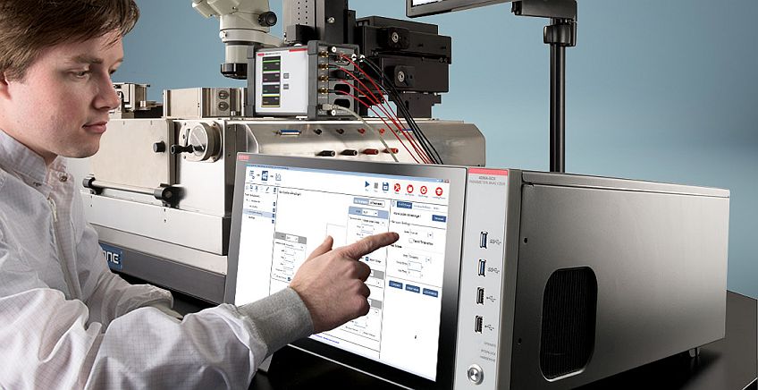
Let’s consider a real use case when a test system has to characterize n-MOSFET transistors for instance. In this application, a test system based on SMUs is used to trace the so called I-V curves, sometimes referred to as the “Output characteristic” or also the “Transfer characteristics”. The gate voltage is programmed to sweep forward and backward (using a SMU, as said) while the drain current is measured (again, using SMUs).
These curves allow to collect useful data to precisely model the activation and deactivation of the transistor conductivity, analyzing when the characteristic reflects linearity or enters a saturation behavior, and how much a self-heating effect can potentially shift these parameters and curves.
When the characterisation refers to modeling the behavior of charge carriers, electrons or holes that jumps between states and modify their mobility according to several conditions, the measurement system connects to the DUT in a four-wire (or remote sense) configuration, and uses triax cables. Looking at the triax cable connection in a four-wire configuration, the total length corresponds to the sum of the Force Hi and the Sense Hi cable lengths.
Based on the capacitance/meter (pf/m) specification of the triax cable, the capacitance of two triax cables having 20m length (10m+10m) connecting the SMUs to the device terminals, can be calculated to be in the range of 2nF for the Guard capacitance and over 6nF for the shield capacitance.
The sensitivity of the SMUs in these cases will be pointless when measuring the transfer characteristic at low current (nanoamps typically) levels, since the capacitance cable loading with cause oscillations. SMUs sensitivity must be combined with the ability to sustain also significant capacitances caused by the cabling load, or the load of any lead that connect the SMUs to the DUT. If this is not the case, the sensitivity will be useless, and produce just noisy oscillating readings.
The ability to identify those conditions when the test capacitance is affecting your measurement is becoming more and more critical. Keithley application engineers are indeed providing valuable consulting in these situations to make sure customers avoid these pitfalls.
Whenever long connecting cables are present in the setup, or switch matrix are between the measurements system and the DUT, or in all cases where the DUT on chuck requires you to enter the range of nanoamps measurements, it’s critical to review the setup and ask for some consulting.
New solutions for the critical ranges
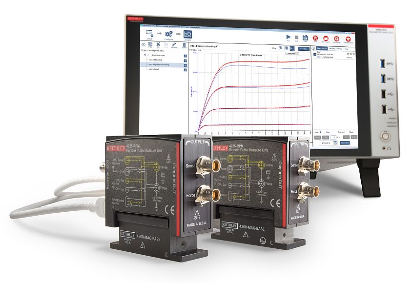
Under these special challenging conditions, it might be necessary to use specific SMUs modules for the measurements. Keithley has released a special version of the SMUs that work in parameter analysis systems like the 4200A-SCS parameter analyzer.
The 4201-SMU Medium Power SMU and 4211-SMU High Power SMU (with the optional 4200-PA Preamp) grant stable low current measurements, even in applications with high test connection capacitance load due to long cabling connections. In fact, these modules can source into and measure a system that is 1,000 times more capacitive than what’s possible today. For example, if the current level is between 1 to 100 pA (picoamp), the new Keithley modules can be stable with as much as 1 µF (microfarad) of load capacitance. In contrast, the maximum load capacitance competitive units can tolerate before measurement stability degrades is just 1,000 pF (picofarad), or 1,000 times worse.
Conclusions
The road towards the optimisation of semiconductors materials for integrated transistors having low contact resistance and special geometries and structures are demanding a continuous improvement of measurements technologies as well. The success of GaN transistors for future power electronics are closely connected to the nanostructures used in their fabrication process. Lower capacitances in the gate width structure raise the problem of considering any other significative capacitances contribution, like the one coming from cabling and connectivity, and overcome problems by improving the SMU ability to handle this for measurements stability.
About the author:
Andrea Vinci is a Technical Marketing Manager at Tektronix, responsible for Keithley Products Portfolio. He got his Electronics Engineering MSc from University of Padova in year 2000, contributing on I.V.I. standard for T&M. He then spent 12 years in technical roles. Since 2011 he joined Tektronix and developed a career in Sales, focusing on Semiconductors and Automotive customers across the EMEA region and specializing in Power Electronics testing solutions. He started a new career chapter joining the Marketing department.

