SmartNICs Drive Greater Efficiency in Data Centers

By: Rita Horner, Program Manager at the Solutions Group, Synopsys 

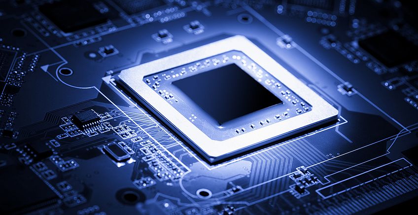
Super-fast data transfer and efficient data processing form the backbone enabling a wide array of modern applications based on hyperscale data centers. Demand for insatiable bandwidth continues unabated and Ethernet speeds have reached 400G/800G bits per second, driven in large part by hyperscalers. These high data rates take a toll on server application processors. This is where network interface cards (NICs) come in. NICs support communication between computers in a system by converting data packages to signals that are spread throughout a network.

Thanks to their programmability and hardware acceleration capabilities, SmartNICs bring flexibility and efficiency to data center networking, storage, and security. By offloading various routine tasks, SmartNICs free host server CPUs to focus on core application processing functions. This article, originally published in the “From Silicon to Software” blog, examines how SmartNICs are supporting our increasingly digital world, emerging data center infrastructure trends, and electronic design automation (EDA) and IP technologies that can help you keep up with the evolution.

Understanding the Intelligence of SmartNICs

As network speeds increased from 1G to 10G to 112G SerDes and Ethernet speeds from 25G to 100G to 200G/400G and, now, 800G, the thinking about hardware architecture has shifted. A peek inside a traditional data center architecture would reveal CPUs, memory, storage, and network components. In recent years, a consensus has formed around the thought that general-purpose CPUs are no longer the best place to run infrastructure functions. A lot of overhead is required to support functions like hypervisors, routing, and load balancing, as well as IO-intensive security functions like deep packet inspection and data storage encryption/decryption.

Some hyperscalers have estimated that around half of CPU cycles are consumed by non-revenue-generating infrastructure tasks. SmartNICs can take on much of the heavy lifting, freeing CPUs to focus on revenue-generating application processing. The intelligence of SmartNICs comes from their programmability, along with their hardware acceleration capabilities. Bringing together wired networking and computational resources on a single card, SmartNICs feature their own on-board processor, accelerators with a custom ASIC implementation, or an FPGA and high-speed memory and IOs.

Integrating intelligence into these networking components has evolved to accommodate changes in data center bandwidth requirements. Initially, there was a focus on offloading infrastructure functions away from the host server CPU. Then, platform functions like cloud technologies were offloaded, from hypervisors to virtual machines, containers, and then microservices. Now, we’re seeing demands for application acceleration; for example, the speeding up of tasks such as video transcoding, encryption/decryption, and packet processing. CPUs can’t support the packet processing demands at today’s highest line rates, so offloading to programmable hardware, in the form of SmartNICs, makes sense.

Data Center Infrastructure Trends

With many potential use cases, what’s the right mix of components for a SmartNIC? Well, there really isn’t a one-size-fits-all approach. Data processing units are at the heart of SmartNICs, and can contain components for programmable compute, network protocol management, security, and storage. For some data centers, a few processor cores are perfect because they’re mainly used for virtual machine management. For others, more than a dozen processor cores are needed to run, say, an entire Linux operating system instance. Looking ahead, here are a few data center infrastructure trends to consider to ensure that your SmartNICs will serve you well into the future as networking traffic continues to grow:

  • The infrastructure of the future for SmartNICs is a disaggregated one, based on four types of die or chiplets: a CPU subsystem, IO subsystem, accelerator ASIC, or FPGA and optionally integrated memory, such as high-bandwidth memory (HBM). Disaggregated dies, or chiplets, support power and area goals while providing the flexibility and product modularity to address different needs in a single package. By comparison, a monolithic approach results in a large, complex chip that comes with yield and time-to-market risks as well as high costs.
  • In a disaggregated die approach, high-speed connectivity between the components is essential to ensure smooth and fast data transfer. High bandwidth, power efficiency, and low latency are key criteria to meet. Universal Chiplet Interconnect Express (UCIe) is emerging as an answer.
  • For main deployment of SmartNICs in every server, the hardware needs to be integrated seamlessly in an open-standard software stack and should be able to run an open network operating system (NOS). Ideally, infrastructure functions are deployed as pre-built containers with APIs that plug into the rest of the software stack layers.

Data center architectures are continuing to evolve to meet ever-increasing bandwidth demands. As such, reliability, security, and interoperability of their IP blocks remain critical for SmartNICs, given their important role in the smooth flow of data traffic. This is where Synopsys can help, with our comprehensive portfolio of advanced IP at different process nodes along with our broad array of multi-die design and verification solutions.

On the IP side, we offer:

  • Die-to-die interfaces including 112G XSR PHY and controllers
  • ARC processors for networking applications
  • Foundation IP including low-latency embedded memories with standard and ultra-low leakage logic libraries
  • Memory interfaces including DDR and HBM PHYs and Controllers
  • Standards-based security IP including hardware secure modules with root of trust, interface security modules, cryptography, and security protocol accelerators
  • Accelerators including DSP
  • Cache coherent expansion including CCIX/CXL controllers, inline AES cryptography, and PCI Express® PHY and Controller
  • Network interfaces including Ethernet Controllers and PHYs for speeds up to 800G.

On the design and verification side, we offer technologies to accelerate the development of multi-die designs, such as our comprehensive and integrated 3DIC solution, which encompasses architectural planning, silicon engineering, 3D system design, verification, test, co-packaged optics, silicon lifecycle management, signoff/system analysis, and IP. In addition, our virtual prototyping tools can help you determine parameters such as the right mix of processor cores and the ideal accelerator for your design. We have design services support, too, to assist with SmartNIC design and/or IP integration and verification.

Summary

Our digital world revolves around high volumes of complex data. To ensure an array of swift and seamless transactions online and in the cloud, data center architectures are moving to a composable model, where homogeneous networking, storage, and compute resources are connected via pluggable optical modules (and co-packaged optics merging electronic and photonic components in the future). In this environment, SmartNICs take the load off of primary compute resources, allowing them to focus on core application processing. While NICs have been around since the mid-1980s, their increased intelligence has made them indispensable for today’s hyperscale data centers. Successful mainstream deployment depends on integration of multi-vendor hardware into industry-standard, open-source software stacks.

The Continued Importance of Unified Power Format

By: Nikhil Amin and Harsha Vardhan, Verification Group, Synopsys

As chip design sizes increase, so does the total power consumption driving its operations. To meet with the increasing intelligence and power-management flow required by modern applications, system on chip (SoC) designers and verification engineers need comprehensive solutions that leverage low-power design techniques to enable fine-grained power management. Over the years, the Unified Power Format (UPF) standard, intended for specifying and verifying power intent of integrated circuit (IC) designs, has advanced and created a wide range of opportunities.

However, for low-power cells like hard macro, RAM cell, or PAD, the connectivity of low-power control signals remains ambiguous. In this article, which was originally published on the “From Silicon to Software” blog, you’ll  learn about the basics of UPF, its importance in the power landscape, how to expand low-power signoff with custom mechanisms, and how to take power-managed designs to the next level.

The History of Unified Power Format (UPF)

As development teams prioritized energy efficiency and adopted low-power approaches, they found difficulties in the specification, implementation, and verification of power management structures. Prior to today’s era of standardization and automation, they didn’t have many resources to solve design problems. The nonprofit organization Accellera Systems Initiative launched UPF for the EDA industry to enable low-power design and verification.

The organization presented it to the Institute of Electrical and Electronics Engineers (IEEE), which published the UPF standard in 2007. Since IEEE’s introduction of the standard, UPF has served as a North Star for chip designers tackling low-power, energy-efficient electronic systems and SoCs. Over the last nine years, new iterations of UPF have been published to advance alongside semiconductor technology enhancements.

Using UPF in Designs

UPF outlines design power intent, specifying control signals, routing, block configuration, and more. Its backbone is the scripting language — Tool Control Language (TCL) — which enables automation for design software, providing specific recommendations to meet low-power standards. On average, development teams report more than a dozen significant challenges related to implementation, specification, and verification of structures.

With UPF, the ability to determine the intended design operation in terms of power management has proven to be effective in overcoming these challenges. Successful implementation of low-power semiconductor designs includes checking UPF descriptions and verifying UPF against the design at multiple stages in the project. Typically, low-power design involves standard control signals such as:

  • Isolation enables
  • Clocks, resets
  • Save, restore, and retain
  • Power switch enables, acknowledgement

UPF designs the standard specifications for these control signals that are distributed traditionally through a power management unit. The most common issues that design teams encounter with low-power signals include complex logic connectivity, incorrect buffers, retimed flops for high fanout net handling, blocked control paths, and swapped connections. A UPF file specifies several key attributes for a low-power design, including:

  • Power supplies: supply nets, supply sets, power states
  • Power control: power switches
  • Level shifters and isolation cells
  • Memory retention strategies and supply set power states
  • Power states and transitions
  • Power/ground pin type

As SoC designs evolve and include more logic functions to meet advanced requirements, the use of complex macros and memories are becoming more common. These cells can have their own low-power modes and functionality which adds unique complexities to the design flow, since the primitive connectivity specifications within UPF are insufficient to meet the verification requirements and architectural-level specifications.

Expanding Low-Power Signoff: UPF and Beyond

Typically, once the initial steps for low-power design are conducted — selection of low-power components, system simulations, UPF, and register transfer level (RTL) coding — designers move to the verification phase, which requires a comprehensive toolkit with several capabilities. The initial step is static power verification and exploration, ensuring the inputs to the design flow (RTL, UPF, and SDC) are structurally and syntactically correct.

Designers need to conduct Lint and CDC checks to make sure the RTL is clean. UPF and SDC checks can be then conducted concurrently with the RTL checks — but a tool that can run these checks and perform power analysis to ensure the design functions properly is key. Software-driven power analysis comes next. For emulation-based low power flows, it is important for chip designers to ensure that peak windows for the design’s power profile are used and leveraged to generate waveforms that estimate power.

The power implementation phase includes several steps for power estimation, logic synthesis, and generating a netlist. Once the checks are complete, the final physical components are placed and routed. During the final step – signoff – designers must ensure that the connections and changes made to the netlist and UPF are consistent and clean, and the power intent is preserved.

Over the years, UPF has grown by incorporating several advanced capabilities. These range from power-intent specification process simplification to power-management flow alignment requirements of IP-based SoC designs. Verification of low power control signals by leveraging control signal connectivity of typical low-power cells such as isolation, retention, and coarse grain power switch within UPF.

Open Issues in UPF

However, for certain low-power cells, such as hard RAM and hard macro, the connectivity of low-power control signals is unclear. This makes verification a complex and manual process often leading to costly bug escapes. Simulation can identify some of these issues but is contingent on a robust simulation environment and corresponding debug capabilities. It also occurs very late in the verification cycle increasing the cost of the verification.

Cases where UPF does not have a way to define specification:

  • While UPF is extensive, the control signal connectivity for low-power cells such as RAM and hard macros remains undefined. Chips are often designed with several RAM cells, and their architecture within the chip is critical to define memory controls and enable low-power optimization features such as sleep and retention enablers. During the design process, engineers frequently rely on simulation to find connectivity issues and other power-related bugs. However, simulations take days and are typically time-intensive procedures.
  • Hard macros present a similar problem. They are often several blocks built into the chip’s design and internally isolated. UPF doesn’t provide checks for internal isolation control or polarity for internally isolated pins.
  • In addition, it is also important to verify an IP-level control signal’s connectivity to the correct SoC signal when the IP is integrated into the SoC to ensure accurate verification at the SoC level. Currently, UPF does not have a mechanism to define the specification for this connectivity.
  • Power state table (PST) dependent isolation enable checks is another area where the Low Power Architect usually defines how the isolation enable signal and its sense are related to a supply. If isolation enable becomes active or inactive in the wrong power state table, then it can propagate corruption or clamp value towards power-on logic and that may not be intended in a PST.

To support the increasing demands of advanced power management from many of today’s electronic products, it is critical to have a comprehensive low-power verification tool that validates the final design functions accurately and can accomplish all of the phases for UPF and RTL checks, power analysis, and signoff. For more information on UPF and pre-empting low-power issues, watch this webinar.

Tackling the Power Monster with UPF Checks Throughout the Design Process

Given the nature of low-power design architectures and behavior, verification and signoff for low-power designs have become more challenging compared to always-on designs. As you’re evaluating verification technologies, consider solutions that are capable of extensive, low-noise reporting, filtering, and waiving to help simplify and also expedite complex, low-power verification signoff flows. Equipped to fully analyze chip performance and capabilities, you can be in a solid position to find and solve low-power bugs faster.

To address the RAM cells, a solution that allows you to quickly conduct full connectivity checks and identify potential problems can mitigate resource costs. As for the hard macros, a solution that allows you to specify control and polarity for these internal components can address the associated challenges.

The Synopsys VC LP™ static low-power verification solution enables all UPF checks, such as scans for power intent consistency, architecture at RTL, structural and power and ground (PG), and functionality. VC LP is a multi-voltage low-power static rule checker that allows developers to validate UPF low-power design intent quickly and accurately. It also features hierarchical power state analysis, power state table debug, and Synopsys Verdi® debug. VC LP also provides solutions for hard macro and RAM cells that UPF doesn’t include.

The platform includes over 650 checks — covering electrical and architectural evaluations — and offers full-chip performance and capacity for comprehensive signoff. It allows users to conduct checks at every step of the chip design process from register-transfer-level (RTL) to post-synthesis and post-place-and-route PG netlist. VC LP offers predictive checks for designers to identify potential implementation problems, allowing for discovery and remediation earlier in the process, as well as providing support for multiple hierarchal flows, such as Black Box and Extracted Timing Models (ETM).

As low-power design continues to become an increasingly important priority and more devices connect to the internet, chip developers will have to keep pace with demand. Design teams will need to prioritize low-power designs and employ advanced power management techniques to operate across all power states going forward.