Tan Reverses Course; Slams Intel’s Former Management

Photo above: Lip-Bu Tan. Leading Intel’s broad restructuring plan

Intel CEO Lip-Bu Tan presented his new vision and roadmap for the company Thursday, marking a dramatic departure from the direction taken by Intel in recent years. Tan is spearheading a sweeping operational and cultural restructuring, which includes massive layoffs, the cancellation of mega-projects in Europe, and a sharp cut in development budgets.

Initial reports of Tan’s cost-cutting strategy emerged when he took the reins in April 2025, but with the release of Intel’s Q2 report this week, the scale became clear: the company officially confirmed the largest layoff in its history, which will reduce Intel’s workforce by approximately 15%.

The restructuring plan includes cutting around 24,000 jobs. By year-end, Intel will employ about 75,000 people. The initiative aims to slash operating expenses to $17 billion in 2025 and $16 billion in 2026. Layoffs are already underway, with reports surfacing in recent weeks of business unit closures and staff exits. In Q2 2025, Intel posted $12.9 billion in revenue and a staggering GAAP net loss of $2.9 billion. The company also issued a disappointing Q3 forecast: revenue of $12.6–13.6 billion with zero adjusted earnings per share.

18A Failed, Servers Were Complex and Pricy

In the earnings call with investors and analysts, Tan delivered scathing criticism of the company’s previous management. “We have a lot to fix to move this company forward,” he said, referring to the failed 18A process node, once considered Intel’s flagship engineering initiative. “We’ve learned a lot from the mistake we made with 18A. We’re applying those lessons now to 14A,” he added. Tan emphasized that 14A investments would only proceed if there’s tangible demand: “I will invest only when I’m convinced the returns are there.”

He was equally blunt about the company’s server processor strategy, which focused on multi-core, multi-threaded chips with dozens of cores and hundreds of threads—regardless of actual market demand. “That approach led to overly complex and expensive CPUs whose performance didn’t justify the cost,” he said. “We are now shifting to a leaner, more focused product line that addresses real customer needs. I will not greenlight chips just because we can build them—only if the market justifies it. I’m fixing the mistakes made in recent years.”

CEO Will Personally Approve All Major Silicon Designs

Tan said Intel still maintains a strong position in the traditional server market. “We’re seeing healthy demand, but we need to improve performance-per-watt for our hyperscale server CPUs,” he explained. “I’ve already taken steps to undo mistakes in multi-threading architecture and am now in the process of bringing in new leadership for our Data Center Group. Expect announcements in the coming months.”

He added: “My directive for future silicon designs is clear: products must feature clean, simple architectures and better cost structures. From now on, every major CPU design will require my personal review and approval before tape-out. This will enhance execution speed, sharpen our focus, and reduce development costs.”

A Software-First Shift in AI Strategy

One of Tan’s most significant announcements was a major strategic shift in Intel’s approach to software, particularly in artificial intelligence. “In the past, we approached AI with a narrow focus on silicon and training—without building an integrated hardware-software stack,” he said. “Our AI strategy must now center on the x86 CPU architecture and Xe GPU architecture, but we must rise to a higher level of abstraction—offering full-stack solutions that include both hardware and software. This is an area where Intel was weak or entirely absent. Under my leadership, that will change.”

“To be the preferred computing platform, we need to deeply understand the most important computing trends and respond with an integrated approach—developing both software and silicon. In the coming months, we’ll provide more details on our efforts to build unified AI capabilities across hardware and software. It will take time, but it’s essential if Intel is to remain relevant in the next computing wave.”

“An Engineering Vision With No Commercial Spine”

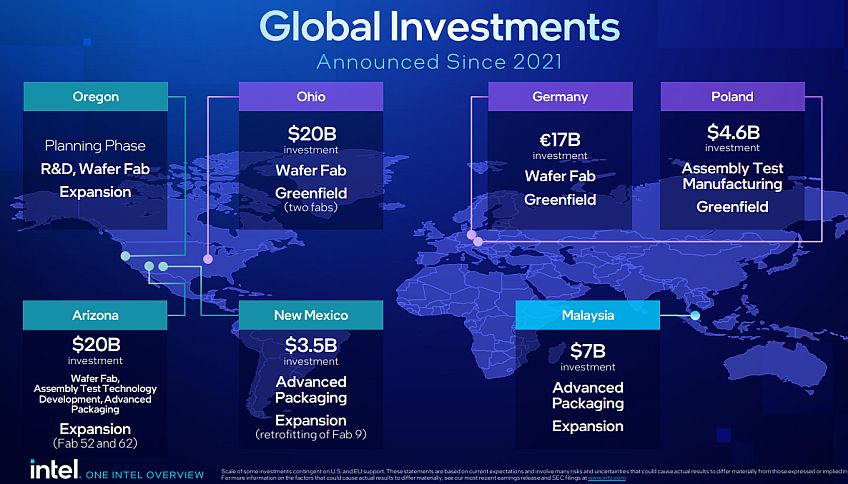
At the core of Tan’s critique was the previous CEO’s manufacturing strategy, which centered on building massive fabs for the Foundry Services division in Ohio, Germany, Poland, and Costa Rica—before securing sufficient customers. “We need to build manufacturing capacity wisely and cautiously, aligned with customer demand and business needs,” Tan said. “The investment in recent years far exceeded actual demand and was done in an unwise and excessive manner. Our manufacturing footprint became too dispersed. Going forward, we will grow capacity only when we have volume commitments and will allocate resources gradually based on milestones.”

Tan reiterated this principle throughout the call: “I don’t believe in the ‘if we build it, they will come’ mindset. Under my leadership, we will build what customers need, when they need it—and we will earn back their trust. That applies both to Foundry projects and to future process nodes. We cannot afford an engineering vision with no commercial backbone.”

Mega Projects Canceled, Engineers Back to Office

Tan’s words have already translated into concrete actions. Intel has canceled the planned €10 billion fab in Germany and the assembly plant in Poland. The Costa Rica site will focus only on R&D, with assembly operations shifting to lower-cost countries like Vietnam and Malaysia. Intel will significantly cut its capital expenditures and slow geographic expansion.

“Our operational metrics already reflect the impact of the changes we’ve started implementing,” Tan said. Going forward, Intel will concentrate resources on just three areas: Foundry-as-a-Service, AI chips, and enhancing existing products. Management layers will be reduced by 50%, and engineers will be required to work on-site at least four days a week. “We need to become a fast, precise, and lean company—like our competitors in Asia,” he said. “This is a strategic shift. We’re not measuring ourselves by near-term earnings, but by our ability to stay relevant over the next two years. The transition to AI and foundry services isn’t a luxury—it’s a necessity.”

Intel and Weizmann Institute Remove the “Speculative Decoding” Bottleneck

Top image: Nadav Timor (right) and Prof. David Harel. Photo: Weizmann Institute of Science

A joint team from Intel Labs and the Weizmann Institute of Science has presented a groundbreaking method for significantly accelerating AI processing based on large language models (LLMs). The research was showcased this week at ICML 2025 in Vancouver, Canada—one of the world’s top AI and machine learning conferences. The paper was selected for oral presentation, a rare honor granted to only 1% of the approximately 15,000 submissions.

The work was led by Prof. David Harel and PhD student Nadav Timor from the Weizmann Institute, in collaboration with Moshe Wasserblat, Oren Pereg, Daniel Korat, and Moshe Bartchansky from Intel, along with Gaurav Jain from d-Matrix. While LLMs like ChatGPT and Gemini are powerful, they are also slow and resource-hungry. As early as 2022, the industry began exploring ways to speed up inference by splitting tasks between different algorithms. This led to the emergence of Speculative Decoding, in which a smaller, faster model “guesses” the next output tokens, and the larger model only verifies the guess instead of computing it from scratch.

A Fast, Lightweight Helper Model

How does it work? In the standard process, LLMs must compute huge operations for every word they generate. For example, to complete the sentence “The capital of France is…”, a model might generate “Paris”, then read “The capital of France is Paris” and compute again to generate “a”, then once more to generate “city”. In total, it performs three heavy compute steps for three words.

With speculative decoding, a fast auxiliary model first drafts the entire phrase—“Paris”, “a”, “city”. Then the larger model checks the full draft in a single validation step. If the guess is correct, all three words are accepted, drastically reducing processing time.

From right to left: Moshe Wasserblat, Oren Pereg, Daniel Korat, and Moshe Bartchansky. Photo: Intel

The Bottleneck That Held the Industry Back

Although speculative decoding has been known for over three years, real-world adoption has been difficult. That’s because LLMs don’t truly “understand” words—they operate based on statistical relationships between tokens. Each model develops its own internal “digital language” of token IDs. For example, the word “apple” might be token #123 in one model and #987 in another.

Until now, speculative decoding only worked when both models (large and auxiliary) used the exact same tokenizer and architecture—usually only possible if they were built by the same company. Developers couldn’t simply pair any fast model with any LLM; they were locked into specific ecosystems.

This created a major bottleneck. The Israeli team overcame this with a new class of algorithms that decouple helper models from LLM architectures, making them cross-compatible across platforms, vocabularies, and companies.

A Surprising Solution to the Compatibility Problem

To bridge this gap, the researchers developed two key techniques. First, an algorithm that enables an LLM to translate its “thoughts” into a language understood by other models. Second, an algorithm that ensures both the large and small models rely primarily on token cognates—tokens with equivalent meanings across different token vocabularies.

“At first we feared that too much would get ‘lost in translation’ and the models wouldn’t sync,” said Nadav Timor, a PhD student in Prof. Harel’s lab and lead author of the paper. “But our fears proved unfounded.”

According to Timor, the algorithms achieved up to 2.8× speedups in LLM performance—resulting in dramatic compute cost savings. “This makes speculative decoding accessible to any developer,” he said. “Until now, only companies with the resources to train custom small models could benefit from these techniques. For a startup, building such a model would have required deep expertise and significant investment.”

Now Available on Hugging Face

The new algorithms have already been integrated into the open-source platform Hugging Face, making them freely available to developers worldwide.

Read the full research paper:
https://arxiv.org/pdf/2502.05202

RealSense Spins Off from Intel, Led by an Israeli Team

[Image: RealSense D435 depth camera. Source: RealSense website]

RealSense, formerly a division within Intel focused on depth-sensing technology, announced today (Friday) that it has officially completed its spin-off from the tech giant and become an independent company. Alongside the transition, RealSense closed a $50 million Series A funding round, led by an undisclosed private semiconductor-focused venture capital firm, with participation from strategic investors, including the investment arms of Intel and MediaTek.

As an independent company, RealSense will focus on developing AI-powered smart vision systems, primarily for the robotics, biometrics, and access control markets. Nadav Orbach has been appointed CEO, following nearly two decades at Intel. Orbach joined Intel in 2006 as an architecture engineer in its Israel development center and later specialized in computer vision and intelligent sensing. He held several senior leadership roles, spearheading the development of depth, facial recognition, and biometric systems. Most recently, he served as Vice President at Intel, leading the Incubation & Disruptive Innovation division focused on advanced projects in AI, robotics, and vision. Orbach sees the spin-off as a unique opportunity to accelerate market expansion. “Our independence will allow us to move faster, innovate bolder, and respond more flexibly to a rapidly evolving market,” he said in a press release.

Israeli R&D at the Core

RealSense began as an internal Intel development group in the early 2010s and was officially launched as a brand in 2014. Over the years, Intel acquired several companies specializing in facial and motion recognition technologies—among them Israeli startup Omek Interactive and InVision Biometrics—to enhance its 3D and computer vision capabilities. At one point, Intel even integrated RealSense technology into consumer cameras and laptops. However, in recent years the division was scaled back, with some operations halted or refocused. The spin-off marks a return to independent growth for the brand.

The company’s headquarters is located in Santa Clara, California, while R&D centers operate in various locations, including Israel, where most of the engineering team—originally formed under Intel—remains. Manufacturing is primarily carried out in Thailand and other parts of Asia. RealSense’s R&D efforts will be led by Guy Halperin, who has been appointed VP of R&D after years of leading Intel’s computer vision teams.

New Camera and Global Growth

Recently, RealSense launched the D555 depth camera, which supports Power over Ethernet (PoE) for simultaneous power and data transmission through a single cable. The device features a Vision SoC with built-in AI capabilities and is designed for use in robotics and security systems. According to the company, RealSense products are already integrated into over 60% of the world’s autonomous robotics systems. Customers include humanoid robotics company Unitree Robotics, Swiss robotics firm ANYbotics, and Fit:Match, a company specializing in augmented reality apparel fitting.

RealSense says it has more than 3,000 active customers worldwide and positions itself as a key provider of robotic vision systems and high-precision biometric solutions. The company maintains global partnerships for manufacturing and distribution and is preparing for further expansion across Asia, Europe, and the United States.

The spin-off comes amid rapid growth in the global robotics and biometrics markets. Demand for autonomous and humanoid robots is expected to rise by tens of percentage points annually, while the need for secure, reliable facial recognition systems is peaking due to emerging applications in transportation, healthcare, and security.

Intel to upgrade Fab38 with $15b Investment

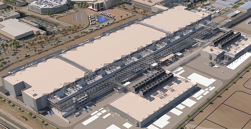
Photo above: Simulation of the future Fab38 in Kiryat Gat, Israel

Israel’s Government and Intel have reached an agreement to expand Intel’s Fab38 in Kiryat Gat, approximately 40 Km from Gaza, where it has an existing chip plant (Fab28). Intel Israel announced an expantion plan of $15 billion in Fab38 planned to be completed within 4-5 years. It will bring the total investment in this fab to $25 billion and enable it to produce advanced semiconductors based on Extreme ultraviolet (EUV) lithography process.

The government of Israel will grant Intel with $3.2 billion worth of incentives. The new fab is expected to create thousands new jobs and to have a major role Intel’s global IDM 2.0 strategy. Intel Israel was founded in 1974 in Haifa, as Intel’s first development center outside the USA, and in 1981 the first factory outside the USA was established in Jerusalem. Today, Intel Israel is the largest private employer in the Israeli hi-tech sector with 11,700 direct employees plus additional 42,000 in indirect employment.

Along with its leading manufacturing facility In Kiryat Gat, Intel operates  three development centers in Haifa, Petah Tikva and Jerusalem, focused mainly on the development of new Processors, Connectivity and Networking technologies, Artificial Intelligence and Cyber Security solutions. During 2022 Intel Israel’s export totalled $8.7 billion representing 5.5% of the hi-tech exports from Israel.

In an interview with Fox Business last week,  Intel CEO, Pat Gelsinger, talked about Intel’s employees during the current Israel-Hamas war. He said: “Many Intel employees in Israel died on October 7, some are being held hostage still in Gaza, and a great many are on reserve duty. But Israelis are the most resilient people on earth. They have not missed a single commitment despite the conflict. That’s why we believe so deeply in them.”


The Financial Reality behind Intel’s IDM 2.0

Photo above: Intel’s Fab 34 in Leixlip, Ireland. $200 million for each EUV Lithography machine

In March 2021, Intel embraced the IDM 2.0 strategy and established Intel Foundry Services as the strategic wing that leads multi-billion dollar in investments throughout Europe and the USA. When this move was first announced, it was seen as a direct threat to TSMC – the world’s largest semiconductor contract manufacturing services provider. This was mainly due to Pat Gelsinger, Intel’s CEO and the shaper of IDM 2.0 strategy, stating multiple times that Intel’s goal is to become the world’s most prominent manufacturing services provider.

The idea seemed unreasonable: why would a genuine semiconductor manufacturer who sells their own processors for high-profit margins shift to another business model – a manufacturing services provider with much lower profit margins? The investors also did not find the idea exciting. In March 2021, Intel’s shares were traded at $64 on NASDAQ. Currently, the shares are worth $35.5 with a market cap of $149 billion.

However, Techtime’s visit to Intel’s new factory in Ireland, Fab 34, reveals that the reason behind the new move is technological rather than merely business. To be more precise, the enormous cost of shifting to advanced manufacturing processes.

€17 billion and five years to set up

Last week, Intel inaugurated Fab 34 in Leixlip, Ireland, which brings Intel 4 technology (equivalent to 7nm) to Europe. It is also the first use of EUV (Extreme Ultraviolet) technology in high-volume manufacturing (HVM) in Europe. The construction of the new fab had began in 2019 and had required €17 billion investments. To provide a point of comparison, Intel operates 3 more fabs in its Leixlip campus that use older technologies, and these factories cost a combined total of €13 billion.

It means that building a fab with the latest technology, such as EUV lithography machines, would be a significant financial undertaking. Industry experts suggest that a factory like this would require 10-20 EUV lithography machines, which are only produced by the Dutch company ASML. Each EUV lithography system costs approximately $200 million.

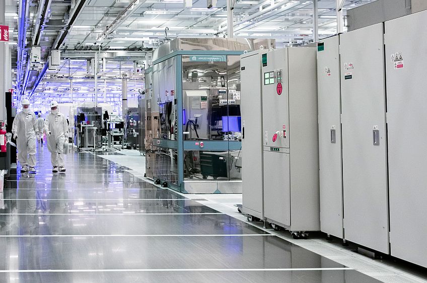
Inside Fab 34 in Leixlip, Ireland. Credit: Intel

The construction of the new factory demands using novell chemical materials for the production of RibbonFET transistors, acquiring new and spcialized equipment and process control and measurements, and a significantly larger clean room that meets higher standards. It is improbable that a single company that bears these expenses and only sells its own products would be able to market them at a profitable price. This is why there are only three companies toady active in advanced processes chips: Samsung, TSMC, and Intel. GlobalFoundries was the last independent firm to be involved in this competition, but it withdrew in 2018.

Intel follows Samsung’s model

Samsung, who acknowledged this challenge earlier, developed a business model for producing self-designed chips together with providing manufacturing services to its competitors, such as Apple and Qualcomm. There are also other companies that embraced this approach, although they are not taking part in the advanced technology race. French STMicroelectronics, for instance, has also adopted this approach by balancing production costs by providing manufacturing services to clients like Mobileye.

Intel’s recent move leaves TSMC as the only company solely focused on providing manufacturing services. Currently, TSMC is the primary supplier of advanced chips to Intel’s largest competitors, including AMD and Nvidia. The conclusion is that Intel’s business model does not pose a threat to TSMC, and there is no indication that Intel intends to compete with TSMC. In fact, Intel has taken significant measures to mitigate the risks associated with transitioning to advanced manufacturing processes.

This is crucial if Intel wants to maintain its position as a market leader. During the recent inauguration ceremony in Ireland, Dr. Ann Kelleher, Intel’s VP and general manager of Technology Development, announced that the company is currently developing four new processes: Intel 3, Intel A20, Intel A18, and the cutting-edge Intel Next. Kelleher stated that the company’s goal is to achieve one trillion transistors in a chip by 2030.

Chiplets require an Open Production Floor

The financial revolution is being accelerated by the move towards hybrid components that consist of several Chiplets; each produced using a different process. This shift creates a new business model where modern processors no longer rely on a single CPU chip but instead integrate multiple peripheral chips from other manufacturers onto an advanced substrate that connects numerous tiles.

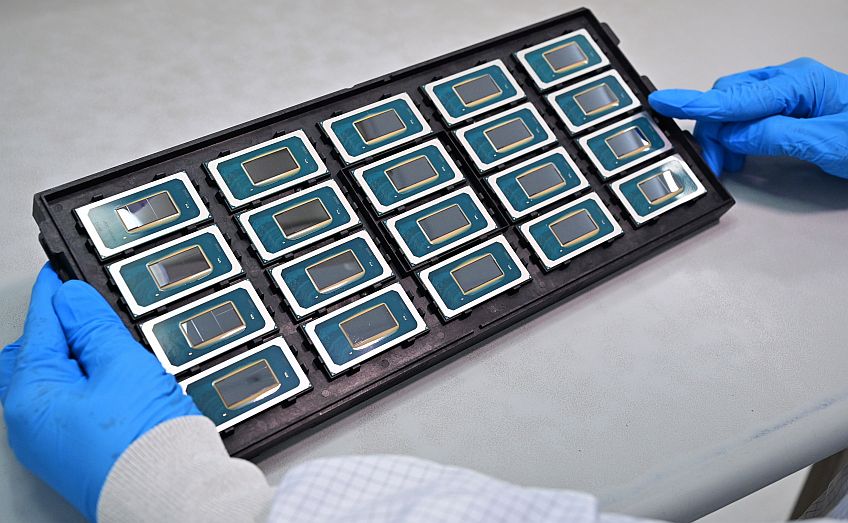
Intel's Meteor Lake chips. 25% made by Intel, %75 by TSMC
Intel’s Meteor Lake chips. 25% made by Intel, %75 by TSMC

This concept is similar to the IP Model prevalent in the Chip Design industry, where any SoC contains the manufacturer’s own proprietary module, along with multiple intellectual property (IP) modules designed by specialized firms. Adopting multi-tile components expands the IP model to the Hardware Level. But it requires to adjust the nature of production lines. Intel, for instance, utilizes this approach in its new chip, Meteor Lake, where 75% of the surface area of the silicon tiles is manufactured by TSMC, and only 25% by Intel.

This shift necessitates the management of an open production floor that can accommodate tiles produced by other manufacturers while producing their own. It also requires the integration of foreign silicon into Intel’s components and the transfer of Intel’s silicon into other vendors’ components, even if they are direct competitors. To achieve this, Intel appears to have chosen a production model that combines self-development and production, side by side with providing manufacturing services.

The Chinese model travels West

Fab 34 project also reveals the importance role of national governments in the semiconductor industry. The cost of transitioning to advanced processes is so high that even major companies like Intel require government incentives. Similar to the Chinese approach, public funding is used to support production firms and boost local industries that rely on advanced technology to create more jobs.

This is why countries like Ireland and Israel are appealing, and why the CHIPS Act and Science Act drive the build-up of new fabs in the US. Intel is also awaiting now to receive approvals from the EU before it will move to the construction phase of its next European fabs: A wafer fabrication facility in Magdeburg, Germany, and an assembly and test facility in Wrocław, Poland.

Translated by P. Ofer

Intel and Tower Announce Foundry Agreement

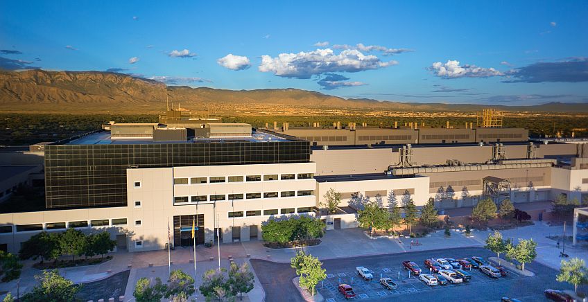
Photo above: Intel’s Fab 11X in Rio Rancho, New Mexico. Credit: Intel Inc.

Less than a month after the termination of a planned merger between Intel and Tower Seniconductor, the two companies announced a largescale production agreement: Intel will provide foundry services and 300mm manufacturing capacity to help Tower serve its customers globally. Tower will utilize Intel’s manufacturing facility in Rio Rancho, New Mexico (Fab 11X), and will invest up to $300 million to acquire and own equipment and other fixed assets to be installed in the facility.

The rearranement of the fab will provide production capacity of over 600,000 photo layers per month. Intel will manufacture Tower’s 65-nanometer power management BCD (bipolar-CMOS-DMOS) and radio frequency silicon on insulator (RF SOI) solutions flows. Stuart Pann, Intel senior vice president and general manager of Intel Foundry Services (IFS) explained during Goldman Sachs Communacopia & Technology Conference this week, that intel had unused capacity in Fab 11X, because it is an older factory for older technologies.

Initial Production in 2025

Pann: “We found a way to do contract manufacturing to take advantage of that extra space. Those older tools that we aren’t using, taking some investment from Tower to finish out the line.” The parties plan to achieve full process flow qualification in 2024, and to begin with full mass production in 2025. Tower CEO Russell Ellwanger said: “We see this collaboration as a first step towards multiple unique synergistic solutions with Intel.”

Tower provides foundry services for Analog semicinductor devices. It offers a broad range of customizable process platforms such as SiGe, BiCMOS, mixed-signal/CMOS, RF CMOS, CMOS image sensor, non-imaging sensors, integrated power management (BCD and 700V), and MEMS. Tower owns two manufacturing facilities in Israel (150mm and 200mm), two in the U.S. (200mm), two facilities in Japan (200mm and 300mm) which it owns through its 51% holdings in TPSCo and is sharing with ST a 300mm manufacturing facility in Italy .

Intel Announced the Termination of Tower’s Acquisition

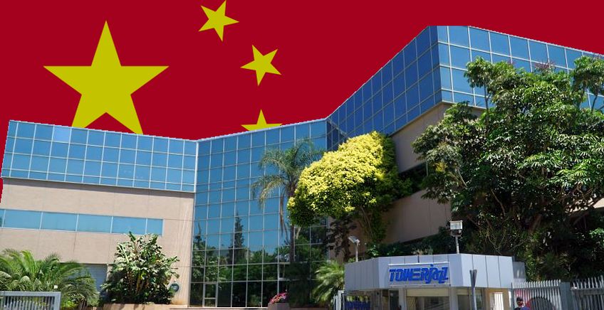
After it had failed to recieve the needed approval of Chinese regulators, , Intel Corporation announced that it has mutually agreed with Tower Semiconductor to terminate its previously disclosed agreement to acquire Tower. On February 15, 2022 Intel and Tower Semiconductor announced a definitive agreement under which Intel will acquire Tower for $53 per share in cash, representing a total enterprise value of approximately $5.4 billion. The aimed to strenthen Intel’s IDM 2.0 strategy to become a leading chip production services provider (foundry).

But during the last 18 months, the US-China tension proved to be a stronger force than Intel’s ambitions, and even after the deal had received across the board approvals, the Chinese authorities made no effort to proceed, and actually waited until it will be clear that no approvel is expexted to be given in the near future. “Our respect for Tower has only grown through this process” said Pat Gelsinger, CEO of Intel, “and we will continue to look for opportunities to work together in the future.”

Russell Ellwanger, Tower Semiconductor CEO, said: “We appreciate the efforts by all parties.  During the past 18 months, we’ve made significant technological, operational, and business advancements. We are well positioned to continue to drive our strategic priorities and short-, mid- and long-term tactics with a continued focus on top and bottom-line growth.”

Tower Semiconductor provides a broad range of customizable process platforms such as SiGe, BiCMOS, mixed-signal/CMOS, RF CMOS, CMOS image sensor, non-imaging sensors, integrated power management (BCD and 700V), and MEMS. It owns two manufacturing facilities in Israel (150mm and 200mm), two in the U.S. (200mm), three facilities in Japan (two 200mm and one 300mm) which it owns through its 51% holdings in TPSCo and is sharing a 300mm manufacturing facility being established in Italy with ST.

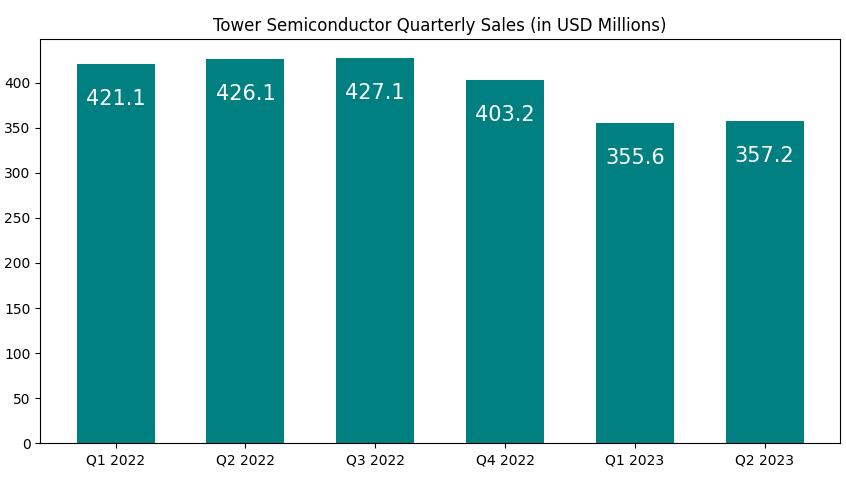
During the last year it faced a slight decline in sales, from $847 millions in H1 2022, to approximately $713 million in H1 2023. until this morning Tower was traded in NASDAQ in valuation of 3.85 billion – 20% below the deal valuation. It means that many investors preculated the deal will fail. Following the deal termination, Tower’s share lost additional 10%, bringing its valuation to approximately $3.5 billion