The Financial Reality behind Intel’s IDM 2.0
3 October, 2023
Intel needs to mitigate the risks associated with the high costs of advanced manufacturing processes. This is crucial if Intel wants to maintain its position as a market leader

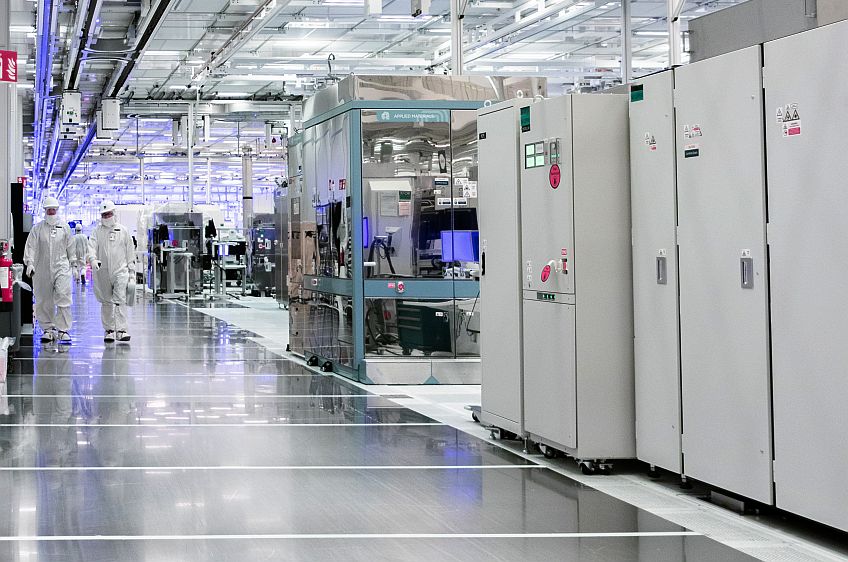
Photo above: Intel’s Fab 34 in Leixlip, Ireland. $200 million for each EUV Lithography machine
In March 2021, Intel embraced the IDM 2.0 strategy and established Intel Foundry Services as the strategic wing that leads multi-billion dollar in investments throughout Europe and the USA. When this move was first announced, it was seen as a direct threat to TSMC – the world’s largest semiconductor contract manufacturing services provider. This was mainly due to Pat Gelsinger, Intel’s CEO and the shaper of IDM 2.0 strategy, stating multiple times that Intel’s goal is to become the world’s most prominent manufacturing services provider.
The idea seemed unreasonable: why would a genuine semiconductor manufacturer who sells their own processors for high-profit margins shift to another business model – a manufacturing services provider with much lower profit margins? The investors also did not find the idea exciting. In March 2021, Intel’s shares were traded at $64 on NASDAQ. Currently, the shares are worth $35.5 with a market cap of $149 billion.
However, Techtime’s visit to Intel’s new factory in Ireland, Fab 34, reveals that the reason behind the new move is technological rather than merely business. To be more precise, the enormous cost of shifting to advanced manufacturing processes.
€17 billion and five years to set up
Last week, Intel inaugurated Fab 34 in Leixlip, Ireland, which brings Intel 4 technology (equivalent to 7nm) to Europe. It is also the first use of EUV (Extreme Ultraviolet) technology in high-volume manufacturing (HVM) in Europe. The construction of the new fab had began in 2019 and had required €17 billion investments. To provide a point of comparison, Intel operates 3 more fabs in its Leixlip campus that use older technologies, and these factories cost a combined total of €13 billion.
It means that building a fab with the latest technology, such as EUV lithography machines, would be a significant financial undertaking. Industry experts suggest that a factory like this would require 10-20 EUV lithography machines, which are only produced by the Dutch company ASML. Each EUV lithography system costs approximately $200 million.
The construction of the new factory demands using novell chemical materials for the production of RibbonFET transistors, acquiring new and spcialized equipment and process control and measurements, and a significantly larger clean room that meets higher standards. It is improbable that a single company that bears these expenses and only sells its own products would be able to market them at a profitable price. This is why there are only three companies toady active in advanced processes chips: Samsung, TSMC, and Intel. GlobalFoundries was the last independent firm to be involved in this competition, but it withdrew in 2018.
Intel follows Samsung’s model
Samsung, who acknowledged this challenge earlier, developed a business model for producing self-designed chips together with providing manufacturing services to its competitors, such as Apple and Qualcomm. There are also other companies that embraced this approach, although they are not taking part in the advanced technology race. French STMicroelectronics, for instance, has also adopted this approach by balancing production costs by providing manufacturing services to clients like Mobileye.
Intel’s recent move leaves TSMC as the only company solely focused on providing manufacturing services. Currently, TSMC is the primary supplier of advanced chips to Intel’s largest competitors, including AMD and Nvidia. The conclusion is that Intel’s business model does not pose a threat to TSMC, and there is no indication that Intel intends to compete with TSMC. In fact, Intel has taken significant measures to mitigate the risks associated with transitioning to advanced manufacturing processes.
This is crucial if Intel wants to maintain its position as a market leader. During the recent inauguration ceremony in Ireland, Dr. Ann Kelleher, Intel’s VP and general manager of Technology Development, announced that the company is currently developing four new processes: Intel 3, Intel A20, Intel A18, and the cutting-edge Intel Next. Kelleher stated that the company’s goal is to achieve one trillion transistors in a chip by 2030.
Chiplets require an Open Production Floor
The financial revolution is being accelerated by the move towards hybrid components that consist of several Chiplets; each produced using a different process. This shift creates a new business model where modern processors no longer rely on a single CPU chip but instead integrate multiple peripheral chips from other manufacturers onto an advanced substrate that connects numerous tiles.
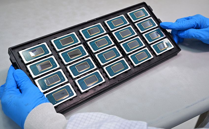
This concept is similar to the IP Model prevalent in the Chip Design industry, where any SoC contains the manufacturer’s own proprietary module, along with multiple intellectual property (IP) modules designed by specialized firms. Adopting multi-tile components expands the IP model to the Hardware Level. But it requires to adjust the nature of production lines. Intel, for instance, utilizes this approach in its new chip, Meteor Lake, where 75% of the surface area of the silicon tiles is manufactured by TSMC, and only 25% by Intel.
This shift necessitates the management of an open production floor that can accommodate tiles produced by other manufacturers while producing their own. It also requires the integration of foreign silicon into Intel’s components and the transfer of Intel’s silicon into other vendors’ components, even if they are direct competitors. To achieve this, Intel appears to have chosen a production model that combines self-development and production, side by side with providing manufacturing services.
The Chinese model travels West
Fab 34 project also reveals the importance role of national governments in the semiconductor industry. The cost of transitioning to advanced processes is so high that even major companies like Intel require government incentives. Similar to the Chinese approach, public funding is used to support production firms and boost local industries that rely on advanced technology to create more jobs.
This is why countries like Ireland and Israel are appealing, and why the CHIPS Act and Science Act drive the build-up of new fabs in the US. Intel is also awaiting now to receive approvals from the EU before it will move to the construction phase of its next European fabs: A wafer fabrication facility in Magdeburg, Germany, and an assembly and test facility in Wrocław, Poland.
Translated by P. Ofer
Posted in: News , Semiconductors
Posted in tags: EUV , Fab 34 , intel , semiconductors


