Panther Lake: The Processor Developed in Israel Alongside Its Manufacturing Process

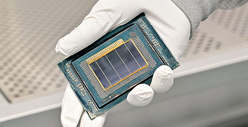
Panther Lake, Intel’s Core Ultra Series 3 processor family, is more than just a new generation of laptop processors. It is also the company’s first product to be manufactured at high volume using the Intel 18A process. As such, it represents a major test of Intel’s ability to return its manufacturing technology to the forefront of the semiconductor industry—and eventually offer it to external foundry customers as well.

In a new 90-minute documentary released by Intel, the program’s managers and engineers describe a development process that began in 2021 and involved thousands of employees around the world. While the film was produced by Intel and frames the project as a success story, it also provides a revealing look at the challenges of developing a processor and the manufacturing process on which it depends at essentially the same time.

Intel’s Israeli development center played a central role in the project. According to the documentary, the product definition process began in a room at the company’s Israeli R&D center, where teams tried to anticipate what the PC market would look like two or three years into the future. The compute tile and CPU cores were developed in Israel, while the graphics technology was developed by teams in Folsom and India. Other components came from additional Intel sites worldwide.

The Israeli executives and engineers featured in the documentary include Zohar Tzaba, vice president and Panther Lake program manager; Yaron Ananki, vice president and head of the Client Development Group; Erik Gihon, senior principal engineer for SoC architecture; Hagai Burstein, product development engineering manager; and Liel Elgarably, client platform integration engineer.

Lunar Lake Efficiency, Arrow Lake Performance

The architectural starting point for Panther Lake was an effort to combine the strengths of Intel’s two preceding processor families.

“Panther Lake is a combination of Lunar Lake and Arrow Lake. We took the best of both worlds and brought them together,” Erik Gihon explains in the film.

From Lunar Lake, Intel carried over power efficiency, battery life and the NPU. From Arrow Lake, it drew performance, scalability and a higher core count. In its largest configuration, Panther Lake features up to 16 CPU cores, compared with eight in Lunar Lake, along with integrated graphics containing as many as 12 Xe cores. Its new performance cores are called Cougar Cove, while the efficiency cores are based on the Darkmont architecture. Both were adapted for the Intel 18A process.

To address a broad range of PC designs, Intel moved from a monolithic architecture to a modular one. The family includes CPU, graphics and I/O tiles of varying sizes that can be combined in three main configurations. An eight-core version is aimed primarily at business laptops. A 16-core configuration with a larger I/O tile adds eight PCIe 5.0 lanes and is designed for PCs equipped with discrete graphics. The flagship version combines the larger processor with integrated graphics featuring 12 Xe cores.

A Manufacturing Process Still in Motion

The project’s unusual challenge stemmed from Panther Lake’s role as the “lead customer” for Intel Foundry’s 18A process. Unlike a product developed on a mature manufacturing node, Panther Lake was designed using evolving versions of the process design kit and frequently updated transistor-performance models.

The product teams had to anticipate how the manufacturing process would behave once it reached maturity and continually adjust the design accordingly.

Intel 18A introduces two major technological changes: RibbonFET, Intel’s gate-all-around transistor architecture, and PowerVia, a backside power-delivery system. In the documentary, Bill Grimm, product engineering manager in Intel Foundry’s Technology Development organization, describes 18A as “a revolutionary process, rather than simply an incremental improvement over the previous generation.”

PowerVia brings power connections closer to the transistors instead of routing them through 14 or 15 metal layers on the front side of the chip. The result is lower resistance, reduced area requirements and potential improvements in both performance and energy efficiency.

The change, however, also forced Intel’s engineers to redesign some of the signal-routing infrastructure. The front-side power-delivery network had previously provided shielding between sensitive signals. Once it was moved to the back of the chip, some metal lines had to be widened and spaced farther apart to prevent interference and preserve clock-signal integrity.

Making Progress With Imperfect Chips

Before the first silicon arrived, Intel tested the design, firmware and software using simulations, emulators and FPGA-based systems. It then began a gradual engineering-sample process. The first ES0 units initially operated at low frequencies. Performance improved through the ES1 and ES2 generations, eventually leading to the B0 revision, which was selected as the production candidate.

Because yields on the new manufacturing process were still limited, Intel developed a method for making use of units that were not fully functional. If only one section of a chip was defective, the unit could be assigned to a validation team that did not require that particular component. This allowed Intel to extract value from nearly every unit coming out of the fab and continue testing despite the limited supply of fully functional samples.

The modular architecture added another layer of complexity. Each processor combines CPU, graphics and I/O tiles produced on different wafers. It was therefore not enough to sort and test each tile separately; Intel also had to match the tiles in combinations that would produce a functioning processor at the required performance tier.

The Bet on B0

One of the project’s most consequential decisions came roughly six months before product qualification. Intel needed to begin building commercial inventory so that hundreds of thousands—and eventually millions—of units would be available at launch. At that point, however, the company still did not know with certainty whether the B0 revision was free of defects that might require another silicon stepping.

The decision was based on the progress of validation, the number of units tested, the status of known defects, yield forecasts and feedback from PC manufacturers. Program executives say it also involved an element of engineering judgment, drawing on the experience of the architects, developers and validation teams.

The gamble paid off: B0 became the production revision of Panther Lake.

At the same time, Intel was working with PC manufacturers on approximately 200 different system designs.

“If all 200 systems had been powered on for the first time at once, our validation and customer engineering teams would have been completely overwhelmed,” says Liel Elgarably.

Intel initially selected a small group of systems and brought them up and validated them together with the manufacturers. Only after resolving the first round of issues did it expand the process to the remaining designs.

The company also dramatically shortened the product-qualification stage. While qualifying the various Alder Lake packages took more than a quarter, Intel had to qualify the entire Panther Lake family within a single month. Findings from the first product were shared daily with the teams responsible for the other configurations, helping them avoid repeating the same tests and encountering the same problems.

For Intel, Panther Lake is therefore more than a new processor. It is the company’s first attempt to turn RibbonFET and PowerVia from laboratory-developed technologies into the foundation of a product family manufactured in tens of millions of units.

The documentary, however, does not disclose yield figures, rejection rates or manufacturing costs. The project’s success will ultimately be measured not only by the fact that Panther Lake reached the market, but also by its real-world performance, the availability of PCs based on the processor, and Intel’s ability to attract external foundry customers to its 18A process.

Watch the full documentary:
Humans are no longer alone online. Organizations need to know who is really in front of them

How do you defend an organization in the AI era? In a special TechTime series, senior leaders from the cyber industry set out the new threats for CEOs and CISOs – and the defensive approach now required.

Guy Tytunovich, founder and CEO of CHEQ

The entire world of identity was built on a single foundational assumption: that on the other side of the interaction is a human being. Usernames, passwords, and two-factor authentication were all designed to verify that a person is who they claim to be. That assumption is collapsing before our eyes.

We are entering an era in which a vast share of digital interactions will be carried out by AI agents acting on behalf of humans – searching, comparing prices, filling in forms, and even making purchases. The implication is that organizations need to learn not just who is in front of them, but what is in front of them.

“Who are you?” is no longer enough

Identity management has to change at its root. Instead of asking only “who are you?”, it needs to answer three questions in real time: is the entity in front of me a human, a bot, or an AI agent; on whose behalf is it acting; and what is its intent?

Agents themselves also need an identity and permissions model, with a clear chain of delegation: who dispatched them, what they are allowed to do, and what reputation they have built up over time.

An organization that can’t tell the difference between a legitimate agent buying on behalf of a real customer and a hostile bot impersonating one will lose twice: the customer, and the security battle.

The threat is at the front door

Security teams today know very well what is happening inside the corporate network, but they are almost blind to what is happening on the digital front line – on websites, in apps, in forms and in APIs.

Think about a bank robbery: the robber comes in through the branch, the place where the money meets the general public. He doesn’t head for the corporate offices of the company that owns the bank. An organization’s digital branch is its website and its app — and that is where many of the new threats operate.

The method of detection has to change too. An attack generated using AI can be polymorphic — every instance of it looks different. So we need to move from detection based only on signatures and rules to detection of behavior and intent.

And when the attacker is autonomous, the response also has to arrive at machine speed. A model in which a human analyst approves every action simply doesn’t survive the pace of events. The SOC of the coming years will run more autonomous defensive agents, and the analyst will shift gradually from being the person putting out fires to the person managing the system.

The danger: a reality that doesn’t exist

The threat that, in my view, gets talked about far too little is actually data contamination. Not one big attack, but a quiet flooding of the internet with synthetic entities.

Armies of bots and agents can open accounts, fill in forms and generate leads, clicks and engagement that look entirely human. The result is that the CRM fills up with people who don’t exist, the analytics describe an audience that doesn’t exist, and business decisions get made on the basis of a fabricated reality. Worse still, the organization’s own AI may end up training on data that was itself created by another AI.

The more organizations open the door to legitimate agents acting on behalf of customers, the greater the incentive for attackers to impersonate precisely those agents.

What should you do tomorrow morning?

If I were stepping into the CISO role tomorrow at a company with 5,000 employees, then before budgets and tools I would map the organization’s digital front door: websites, apps, forms and APIs.

I would ask a simple question: how much of the traffic there is human, how much is automated, and how much of it is already coming from AI agents.

You can’t protect what you can’t see. In the new world, organizations will have to treat non-human entities as full citizens of the identity system too — with permissions, accountability, and the ability to know who sent them and what they are allowed to do.

The next stage is already visible on the horizon: agent authentication. Just as SSL became a standard without which a browser won’t trust a website, we will reach a world in which a business can’t trust an agent without knowing who it is and on whose behalf it is acting.


EWP to develop Digital Twin Platform for Sea Wave Energy Technology

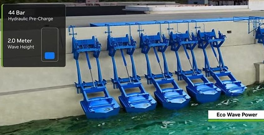
image above: An illustration of a digital model of a wave energy generation system. Source: EWP.

Eco Wave Power Global (EWP) announced that its wholly owned U.S. subsidiary, Eco Wave Power U.S, has entered into an agreement with Germany-based AI engineering GmbH to develop a physics- and data-driven Digital Twin platform for Eco Wave Power’s proprietary wave energy technology. Both Eco Wave Power U.S. and AI engineering are members of the NVIDIA Inception program.

Under the agreement, the companies have commenced Phase 1 of the project, combining advanced physics-based simulation with EWP’s real-world engineering, wave and operational data. The initial phase will focus on digitally modeling how ocean waves interact with EWP’s proprietary floaters. Using AI engineering’s PAMICS simulation technology, the companies will evaluate floater behavior, structural loads and theoretical energy input under different sea conditions.

“For us, AI is an opportunity to fundamentally improve how we understand, design, predict and ultimately operate wave energy systems,” said Inna Braverman, Founder and CEO of EWP. “Phase 1 of this collaboration is therefore very practical. We will model wave loading, floater behavior, structural forces and theoretical energy input, while beginning to develop machine-learning capabilities for forecasting loads and energy yield. Importantly, we will also examine how those models can be transferred to new sites with different wave conditions.”

Digital representation of EWP system

AI engineering is specializes in applied fluid mechanics, numerical flow simulation and high-performance computing. Its PAMICS technology is a particle-based multiphysics simulation framework designed for complex fluid-dynamics and fluid-structure interaction applications. “Wave energy is a particularly challenging engineering problem because it combines complex free-surface fluid dynamics, structural motion, and highly variable environmental conditions,” said Dr. Stefan Adami, Co-Founder and General Manager of AI engineering GmbH.

“Our goal is to create a physics-based digital representation of Eco Wave Power’s system that links high-fidelity simulation with operational data. This approach allows us to better understand energy capture, structural loading, and system behavior across a wide range of sea states. Combining these physics models with ML can support more accurate forecasting, design optimization, and scalable deployment of wave energy technology.”

Michal Braverman-Blumenstyk to Leave Microsoft After 13 Years

Michal Braverman-Blumenstyk, General Manager of Microsoft Israel R&D and CTO of the company’s global Security division, has announced that she will leave Microsoft at the end of 2026, after 13 years with the company. Braverman-Blumenstyk has led Microsoft’s Israel R&D center for the past six and a half years. Microsoft said it will announce her successor at a later date.

Her departure is also significant for Microsoft’s global cybersecurity operations. Braverman-Blumenstyk has effectively held two roles in parallel: leading Microsoft’s broader R&D organization in Israel while also serving in a senior technology role within the company’s global security organization.

Braverman-Blumenstyk joined Microsoft 13 years ago to establish and lead its cloud security group in Israel. She later became one of the founders of the company’s Cloud + AI Security division and, following the consolidation of Microsoft’s security operations, was appointed CTO of Microsoft Security. Over the years, she played a role in developing and launching products that became key parts of Microsoft’s cybersecurity portfolio, including Microsoft Sentinel and Microsoft Defender for Cloud, and was also involved in strategic cybersecurity acquisitions.

As CTO, Braverman-Blumenstyk has focused on identifying emerging technologies and new growth areas for Microsoft’s Security division. In recent years, her responsibilities have also included shaping the company’s security strategy for the AI era. Microsoft is developing, among other technologies, AI agents capable of autonomously performing security tasks, alongside tools designed to secure AI models and agents themselves.

Microsoft’s First R&D Center Outside the US

Microsoft established its Israel R&D center in 1991, making it the company’s first development center outside the United States. Today, it comprises dozens of development groups working across cybersecurity, cloud computing, artificial intelligence, analytics and software products. The center contributes to several major Microsoft organizations, including Security, Cloud & AI Platform, and Experiences & Devices.

During Braverman-Blumenstyk’s six and a half years at the helm, the center doubled its workforce and expanded its operations across six sites in Israel. Over the same period, Israel has become one of Microsoft’s key global development hubs for cybersecurity.

Braverman-Blumenstyk has more than two decades of experience in cybersecurity and holds a master’s degree in computer science from Columbia University, where she specialized in artificial intelligence.

In an email to employees, she wrote: “I’ve had the privilege of leading the Israel Development Center for the past six and a half years, and it is the part of my journey I am most proud of.” She also referred to the period since October 7, highlighting the resilience and perseverance of the center’s employees.

Microsoft has not yet announced who will succeed Braverman-Blumenstyk as head of its Israel R&D center, nor has it said how her global responsibilities as CTO of the Security division will be reassigned.

[Photo: Netanel Tovias]

Effect Meta: Lumus Ramps Up Production

[Pictured: Meta’s Ray-Ban Display glasses. Credit: Meta]

By Yohai Schwiger

Israeli company Lumus, based in Ness Ziona, is expanding its manufacturing capabilities ahead of the next generation of AR and AI glasses. The company has signed a new licensing agreement with Taiwanese manufacturing giant Quanta Computer, under which Quanta will manufacture Lumus’ next-generation waveguides, including the Z-30 2.0 and the new A-Lens family. The new products were designed to be thinner, lighter and less expensive to manufacture, making them better suited for high-volume production of consumer AR glasses.

The agreement comes as the smart glasses market begins to transition from a niche segment into a meaningful consumer category. One of the major milestones was the launch of the Meta Ray-Ban Display in September 2025. Unlike previous generations of Ray-Ban Meta glasses, which featured cameras, speakers and an AI assistant but no display, the new model incorporates a color display into one of the lenses, allowing users to view messages, navigation directions, translations and information generated by Meta AI.

The waveguide used in these glasses is based on Lumus technology. The component enables a digital image to be projected into the user’s eye without obstructing their view of the surrounding environment. According to market research firm TrendForce, Meta initially ordered about 80,000 Lumus waveguides, but later increased the order by approximately 87.5% to 150,000 units in response to demand. In January, Meta also postponed expanding sales of the glasses beyond the U.S. due to limited inventory and stronger-than-expected demand, with waiting lists stretching well into 2026.

A Partnership Spanning Nearly a Decade

Quanta is not a new partner for Lumus. The relationship between the companies began in 2016, when Quanta invested in the Israeli company. In 2017, Lumus completed a $43 million funding round backed by investors including Quanta and Alibaba, and the two companies signed a licensing agreement that same year aimed at bringing Lumus technology into mass production.

Quanta, which generated approximately $68 billion in revenue in 2025, is one of the world’s largest ODM manufacturers, producing computers, servers, AI systems and other electronics for major technology companies. In recent years, it has also expanded its presence in smart glasses. In March 2026, for example, Quanta signed a multi-year manufacturing agreement with Innovega to scale production of its smart glasses.

Lumus also works with another major manufacturing partner, German glassmaker SCHOTT, which manufactures its waveguides at a facility in Malaysia. According to Lumus, the two partners together provide production capacity of more than six million units. More than 200,000 Lumus waveguides have been manufactured and shipped to date for consumer, defense and medical applications, with the company reporting manufacturing yields of more than 95%.

Tiny Mirrors Inside the Lens

Founded in 2000, Lumus develops geometric, or reflective, waveguide technology. The waveguide receives an image from a miniature projector, guides the light through the glass and redirects it toward the user’s eye through an array of tiny reflective surfaces embedded within the lens. At the same time, the user continues to see the real world through the transparent lens.

Lumus’ architecture differs from diffractive waveguides, which use microscopic optical structures to manipulate and direct light. According to the company, its approach provides higher optical efficiency, greater color uniformity and lower light leakage. This allows for a smaller projector and lower power consumption, both critical parameters for devices intended to look and feel like ordinary eyeglasses.

The new generation to be manufactured by Quanta is intended to further address the size and cost constraints of consumer glasses. The Z-30 2.0 provides a 30-degree field of view in a thinner and lighter optical engine, with improved brightness and the ability to directly attach a prescription lens to the waveguide. The A-Lens family will be available with 30-degree and 50-degree fields of view and, according to Lumus, is approximately 50% thinner and lighter than previous generations while being designed from the outset for lower-cost manufacturing.

Lumus initially focused primarily on markets where component cost was less of a constraint. Its technology has been incorporated into Thales’ Scorpion display for fighter pilot helmets, Augmedics’ xVision surgical navigation system and Lenovo’s ThinkReality A6 smart glasses. Its integration into the Meta Ray-Ban Display represents a significant step into the consumer market.

The broader market is now approaching a potential inflection point. TrendForce estimates that global AR glasses shipments will increase 53% this year to approximately 950,000 units. At the same time, the broader success of Meta’s AI glasses portfolio is attracting additional players to the category and increasing pressure to reduce weight, power consumption and component costs. For Lumus, the new Quanta agreement is intended to ensure that its next generation of optics is ready if and when the market moves from hundreds of thousands of glasses to millions of units.

Innoviz Appoints Yoav Har-Even as Chairperson

photo above: Yoav Har-Even

Innoviz Technologies announced that its Board of Directors has appointed Yoav Har-Even, a member of the Board, to serve as Chairperson, effective immediately. Har-Even succeeds Amichai Steimberg, who has elected to step down as Chairperson after leading the Board since the Company’s listing on Nasdaq in April 2021. Mr. Steimberg will continue to serve as a member of the Board.

Har-Even joined the Board of Innoviz in July 2026. Prior to that, he served as President and Chief Executive Officer of Rafael Advanced Defense Systems from 2016 to 2024, where he led the company’s global operations, technology development, manufacturing and international business activities. Prior to joining Rafael, Har-Even served for more than three decades in the Israel Defense Forces, retiring with the rank of Major General (Ret.). Currently he serves also as chairperson of Sindiana Technologies and as a member of the advisory boards of Ondas Holdings and Massivit 3D Printing Technologies.

Innoviz provides LiDAR technology and is serving as a Tier-1 supplier to the world’s leading automotive manufacturers. Its LiDAR sensors and complementary software suite are designed to deliver accurate 3D sensing even in harsh weather conditions. These days Innovi extends its existing sensing solutions into defense, homeland security, industrial, and smart infrastructure markets.

“Mr. Har-Even’s appointment as Chairperson reflects the strategic weight defense and security now carry for Innoviz” said Omer Keilaf, Founder and CEO of Innoviz. “His experience leading Rafael and his years at the highest levels of the IDF give the Board deep insight into this space, strengthening Innoviz’s ability to scale in these markets.” Har-Even added: “Defense and security represent a substantial opportunity for the Company, and LiDAR is becoming a critical sensing layer in areas such as counter-UAS, unmanned ground vehicles, and perimeter security.”

Lately Innovis announced record revenue of $18.1 million in Q2, and is expecting to reach 2026 annual revenue of $67–$73 million. Keilfaf: “Our partnerships with VW, Mobileye, Daimler Truck, and others are on track. W recently announced the development of a LiDAR-based perception stack with a top 10 global OEM. We believe the combination of the automotive market and the defense and security markets has the potential to create a flywheel effect, as we work to become a premier worldwide supplier of best-in-class LiDAR solutions.”

Unique Battle Management Platform

By Roni Lifshitz

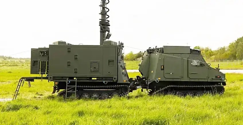
Elbit Systems’ Swedish subsidiary, Elbit Systems Sweden AB, unveiled its Tactical High Mobility Shelter (THMS) system at the DALO exhibition in Denmark. The system serves as a mobile battlefield networking platform designed to support dispersed, digitally connected forces. The project has undergone significant changes. In January 2023, Elbit reported that its subsidiary, Elbit Systems Sweden, had been awarded a contract worth approximately $48 million to supply tactical communications shelters to the Swedish Defence Materiel Administration (FMV). However, over the following three years, key lessons from the war in Ukraine began to emerge, prompting a major transformation of the project. The changes were significant enough for Elbit to publish a dedicated blog post titled “From Static Bases to Mobile Networks.”

In the article, Elbit explains that in its updated configuration, the project reflects a broader shift in the way land forces operate: communications systems, sensors and command capabilities must move as quickly as the forces they support.

“The war in Ukraine has reinforced the need for highly mobile and dispersed operations,” explained Christian Tengelin, Director of Business Development at Elbit Systems Sweden. “The modern battlefield requires units to establish connectivity, operate and relocate very quickly. Remaining in one location for too long can rapidly lead to detection and targeting.”

The War in Ukraine Changed the Mission Requirements

Elbit Systems Sweden employs approximately 120 people. Tengelin said that the scope of the THMS program has expanded considerably. The Swedish Ministry of Defence redefined the system’s intended role, and what began as a project to replace an existing capability in the Swedish Armed Forces evolved into a broader change in the way the Swedish military operates dispersed forces.

“In countries with large territories and long borders, the challenge is not simply moving personnel and vehicles from one location to another. Units deployed across wide areas must remain connected to one another and to higher command levels, while retaining the ability to rapidly deploy sensors, communications equipment and other mission systems.”

The new version of THMS was developed and is manufactured in Sweden, based on a European supply chain. It is designed for operational deployment in harsh environments, including extreme weather and Arctic conditions. The system enables military forces to rapidly establish elevated communications and sensing capabilities without relying on fixed infrastructure or static command posts.

It is equipped with a telescopic mast that can reach a height of up to 25 meters and carry mission payloads weighing up to 100 kg. In practice, it now serves as a multi-mission platform supporting the integration of a wide range of payloads and mission capabilities, including tactical communications, electronic warfare (EW) systems, surveillance and observation systems, electro-optical and infrared (EO/IR) sensors, satellite communications (SATCOM), tactical 5G technologies and high-power laser (HPL) capabilities.

The mast can carry a variety of mission-specific payloads, including communications equipment, ISTAR sensors and Counter-UAS systems. The system operates as a fully self-contained unit with an integrated power-generation system, enabling autonomous operation for up to 24 hours without relying on the vehicle carrying it.

The mast’s automatic deployment mechanism and unique automated guy-wire system allow the THMS to be set up in less than five minutes, while reducing the workload on operators in the field. Notably, it can operate in both crewed and remotely operated unmanned configurations.

Elbit said that future development is expected to move toward higher levels of autonomy—meaning the system could eventually evolve into an almost robotic platform. “Future land operations will depend on the ability to connect dispersed forces, sensors and effectors in real time,” said Tobias Wennberg, CEO of Elbit Systems Sweden.