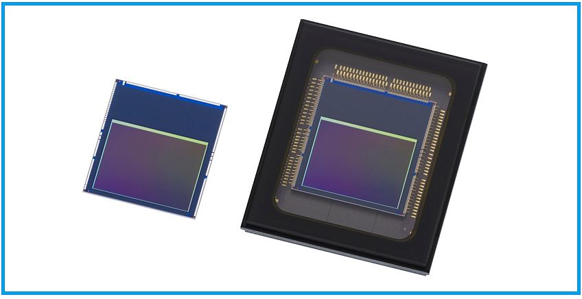
Photo above: Sony intelligent vision sensors IMX500 (left) and IMX501. Both include Altair’s DSP processor
Hod Hasharon-based Altair Semiconductor (owned by Sony) has secretly expanded its operations beyond the IoT sector and entered the Artificial Intelligence (AI) chips market. This came to light last month, when Sony announced new image sensors for smart control systems . The component is built of two chips embedded in stacked configuration inside a single package (Multi Chip Module) consisting of a Sony image sensor, and a DSP processor developed by Altair, which is responsible for a neuronal network inference operations.
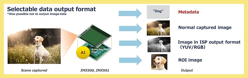
This new family of smart image sensors is currently consists of two components: IMX500 and IMX501. When installed in a security camera, street camera, or other IoT devices, the logic circuit processes and sends only the inference itself to the network center. Thus, it saves considerable processing and communication resources and enables a given device to function as a smart sensor without compromising the privacy of the people being photographed.
A smart camera equipped with the visual-logic sensor can enumerate the number of people in the store and transmit the information without having to send their images to the cloud. It can discern congestion patterns in various complexes, and even track customer behavior in the store – based only on analyzing their movements – and without having to identify the customers themselves.
The images are sent back in a variety of configurations (see below): pure decoded information without visual elements, an image in various formats, or only the relevant visual area. From Sony’s point of view, this constitutes an entrance to a major market characterized by a very large growth. As far as Altair is concerned, this is a very surprising development, since so far the company has focused on communication solutions for IoT devices and not on the development of DSP or artificial intelligence processors.
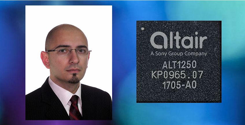
Altair’s core activity is focused on IoT connectivity chips, with its flagship product being the ALT1250 chipset, which includes a modulator and a modem for supporting Cat-M1 standard and the NB-IoT standard. It features an RF front end circuit that supports all LTE bands, an RFIC circuit, a power management unit (PMU), memory, amplifier circuits, filters, an antenna switch, global navigation satellite system (GNSS), hardware-based security, an eSIM circuit and an internal micro controller unit (MCU) that allows customers to develop unique applications.
A new strategy for both Altair and Sony
Sony’s announcement positions it in a massive market and transforms it into ahybrid IoT-image-sensors player. The move can secure orders for Altair in very large quantities. However, it can also hint at a new Altair strategy that can develop in two interesting directions: the first is the integration of ALT1250 technologies into Sony’s future image sensors – alongside the recently unveiled AI processor.
The other direction is independent: integrating the artificial intelligence processor into its next-generation connectivity chip – a kind of ALT1250 reinforced with artificial intelligence. An IoT connectivity chip embedded with artificial intelligence has many advantages – from providing artificial intelligence to ‘dumb’ cameras – thus allowing enhanced communication management capabilities – and even enhancing the current-generation ALT1250 security system.