Augury raised $180M on $1 billion valuation

Augury Company from Haifa has completed a $180M fundraising, based on $1 billion company value. Current round raises the company’s total fundraising to $286M. The round was led by Baker Hughes, one of the biggest global providers of services and equipment for the gas & oil industry, with more than a $20 billion revenues in 2020. Following the investment, Baker Hughes will take a seat in Augury’s board of directors, and will also incorporate Augury’s platform into its operational systems. New investor in the current round is SE Ventures, the corporate venture arm of Schneider Electric.

With $200M in cash, Augury will use it to globally expand its operation and enter new fields such as the energy sector. The company was founded in 2014 by CEO Saar Yoskovitz and CTO Gal Shaul. Company’s headquarters is located in New-York, while its R&D center is in Downtown Haifa. Augury’s platform monitors industrial machines’ mechanical state using various sensors, including vibration, temperature and magnetic sensors.

The information gathered by the sensors is collected continuously, transmitted to the cloud and analyzed by artificial intelligence algorithms combined with operational and mechanical models. The analysis in the cloud compares between the data collected from current machine’s state and historical data regarding current machines and other similar ones. This analysis provides insights regarding abnormal patterns which might indicated machine malfunction, flaw or depreciation. Also, the system produces recommendations as for the optimal methods of locating and fixing the issue. Augury’s customers include Heineken, Tnuva, Danone, Bosch Health, Nestle, Nefco and more.

DustPhotonics new focus: InP Laser for Silicon Photonics

Above: Ronnen Lovinger, CEO of DustPhotonics.

Israel-based DustPhotonics exits its current optical transceiver’s business and is moving to the promising new field of active technologies for silicon photonics. The company announced a new investment, totalling $33 million, led by Greenfield Partners and joined by Intel Capital, Avigdor Willenz (co-founder of Habana Labs), and others. The company also announced it has completed an organizational realignment to support its new business direction: Phasing out its current Transceivers product line to focus its resources on silicon photonics solutions.

As part of this move, Ronnen Lovinger, president of DustPhotonics, has assumed the role of CEO. Ben Rubovitch, the company’s previous CEO, has stepped down and will lead the Business side of the company. “This latest investment and the organizational changes will enable us to take advantage of new business opportunities,” said Ronnen Lovinger. “We are thrilled at the continued confidence of our investors in our strategic direction.”

DustPhotonics high-speed pluggable transceiver

DustPhotonics was founded in 2017 with offices in Modi’in, Israel and Cupertino, California. Currently, it provides high-speed optical pluggable transceiver for datacenters, based on its proprietary AuraDP technology. It seems that it takes its optical alignment technology which is at the heart of AuraDP – into a more lucrative market – InP (Indium Phosphide) Laser to Silicon Photonics integration. “This technology will provide significant value differentiation enabling superior performance to support 800 Gb/s, 1.6Tb/s, CPO (Co-packaged Optics) and future products.”

Softbank Vision Fund 2 takes stake in OurCrowd

OurCrowd, Israel’s most active venture platform [1], today announced that SoftBank Vision Fund 2, will make a $25 million convertible equity investment into the firm. Proceeds of the round will go toward the expansion of the OurCrowd platform, building its investor base and accelerating the identification of high-potential, tech-enabled private companies.

With 140,000 accredited investors from more than 195 countries, OurCrowd is a leading platform providing investors with access to quality venture capital investment opportunities. Rated Israel’s most active venture investor by PitchBook, OurCrowd has invested in over 280 companies and 30 funds.

OurCrowd has achieved record growth in the past year. New registered subscribers added to the OurCrowd platform have soared from 25,000 in 2020 to 75,000 in 2021 so far, representing 300% growth with three months remaining before the end of the year. New investments made this year on the platform will exceed $500 million, representing more than 100% growth in additional annual AUM. More than 50 OurCrowd portfolio companies have achieved exits including Lemonade, Beyond Meat, Uber (Jump), Kenna, Argus, Wave, and many more.

Under the agreement, OurCrowd will also enter into a strategic partnership with SoftBank Investment Advisers (SBIA – Sub-Adviser to SoftBank Vision Fund 2), to consider investment opportunities via OurCrowd’s online venture capital investment platform. The parties will also work with each other to evaluate market trends in a broad variety of sectors including Artificial Intelligence, Quantum Computing, Mobility, Agtech, Cybersecurity, Healthtech and more. The collaboration will also see OurCrowd and SBIA support geographic expansion across their respective ecosystems.

OurCrowd CEO Jon Medved said: “We are excited to be working with SoftBank Investment Advisers, one of the world’s largest technology-focused investors. As a strategic investor with a global reach and a network of market-leading technology companies, they will be a pivotal partner in helping OurCrowd realize our vision of democratizing access to venture capital.”

Yossi Cohen, head of SBIA’s operations in Israel, said: “Softbank has been investing ahead of major technology trends for over 40 years and we believe there is huge, embedded potential in the private markets ecosystem. In OurCrowd, we have an investment partner with the networks and pedigree to help promising Israeli startups to potentially emerge as international tech champions.”

Renesas to Acquire Celeno for $315 Million

Above:President & CEO Gilad Rozen. Photo: Techtime

Renesas Electronics announced it has entered into a definitive agreement to acquire Celeno Communications from Raanana (near Tel aviv) for an amount of US$315 million. The transaction has been unanimously approved by the boards of directors of both companies and is expected to close by the end of 2021. The acquisition significantly enhances Renesas’ connectivity portfolio with the addition of Celeno’s Wi-Fi technologies and software expertise.

Celeno offers advanced Wi-Fi chipsets and software solutions, including the most compact chipset for Wi-Fi 6 and 6E. Celeno has developed a unique Wi-Fi Doppler Imaging technology, that provided local radar functionality using its Wi-Fi connectivity chip. The deal is a part in Renesas’ new connectivity strategy which was also culminated with the US$5.9 Billion merger with Dialog in February 2021.

“Renesas is now strongly positioned to capitalize on the growing opportunities from the massive rise in connectivity and requirements created by today’s increasingly connected world,” said Hidetoshi Shibata, President and CEO of Renesas. In addition to expanding the solution offering, the acquisition also increases Renesas’ engineering and design scale with Celeno’s design center in Israel. Techtime has learned that the new center will develop connectivity solutions for the Automotive industry, including V2X chips.

Celeno was established in 2005 by the President & CEO Gilad Rozen. It received US$140 Million investments from high profile bodies such as Cisco, Samsung and major VCs. Its main competitors are Qualcomm, Broadcom and Mediatek. Most of its 170 employees are located in Israel. During 2020 Celeno shipped 15 million chips to costumers, for total sales of US$37 Million.

“Our depth and strength in connectivity combined with Renesas’ industry leading portfolio of embedded solutions will allow us, together, to open up new growth areas we can target,” said Gilad Rozen.” Renesas will also provide us with the go-to-market capabilities to bring Celeno to a broader range of customers.”

StoreDot to establish a US Hub to accelerate a Solid State battery development

SroreDot Company, the developer of Extreme Fast Charging Battery, is going to open an R&D center in California. This major step is part of the company’s development efforts to create the next generation of its battery, which will be a Solid State one, with extreme energy-density (XED) and will allow for driving range greater in 50% than the current generation. At the same time, the company announced its negotiations with USA-based manufacturers to establish a local battery production line, in order to shorten supply chain for American customers. Currently, company’s batteries are manufactured in China by the local battery manufacturer EVE.

In Solid State battery, the electrolyte, through which ions pass in the loading-unloading process between the electrodes is made of solid material. In the existing Lithium-Ion batteries, the electrolyte is usually made of liquid or polymer-gel. Solid State batteries are considered safer, since they don’t suffer from current batteries’ dangers such as high temperatures flammable or explosion, liquid leakage etc. in addition, the Solid State battery’s capacity should be larger, allowing for higher driving range. The main challenge is to develop a solid material that will be solid at the one hand, and high conductivity at the other hand. Also, the developers have to cope with solid electrolyte’s tendency to crack and be broken.

The Solid State battery is considered to be the Holy Grail of the EV industry, the one that will make electric vehicles cheaper, safer and with higher driving range, soothing range anxiety. Many players at the vehicle industry put a lot of efforts in developing Solid State batteries. One of the leaders in these development efforts is Toyota, lately announced an $13.5 billion investment plan for developing new batteries technologies and production capabilities, to include a Solid State battery. The Japanese manufacturer is expecting to complete the development of the battery in the middle of current decade, although lately admitted that it struggles with some technical difficulties. Among other manufacturers, Ford, BMW, and Volkswagen are all in the race for developing Solid State battery. The American EV manufacturer of Fisker, which has much more limited resources being a start-up company, announced six months ago that it completely cancels its program to develop such battery. 

Ultra-fast charging of EV’s batteries

StoreDot has developed the FlashBattery technology, allowing Li-ion batteries to be charged in only several minutes. This technology is based on NanoDots particles, each at the size of 2 nanometers, characterized by high capacity and integrated in the electrolytic liquid within the battery.

In early 2021, StoreDot has produced the pilot production batch of EV batteries in a plant of the Chinese battery manufacturer Eve Energy. These batteries were used to demonstrate full charge of a two-wheeled EV in just five minutes. At May 2021 StoreDot signed an agreement with Eve Energy, under which it will produce early samples for clients by the year end, and starting at 2024 it will mass-produce the batteries for integrating in various EVs.

Classiq launched its beta version for the quantum software platform

Israeli quantum software start-up Classiq launched lately its proprietary platform’s Beta version which allows, for the first time in the industry, to compose functional algorithms for Quantum computers. The company made the new platform available to several customers, among them a Telecom company, Aerospace Company, financial firm, consulting agency and several academic bodies.

In the next few months, the company plans to expand the beta version access to several dozen customers.  In addition, the company had filed 9 patent applications to the USPTO (United States Patent and Trademark Office) for its IP relating quantum computing software. The applications relate to writing, compiling, debugging and optimizing functional algorithms designed for Quantum machines. Classiq Company was founded in May 2020 by CEO Nir Minerbi, Head of Algorithms Amir Naveh and CTO Yehuda Naveh. The R&D team currently includes 25 people.  

In recent years, there has been a significant breakthrough in quantum computing, and many technology giants are building powerful quantum computers that are capable, at the level of hardware, of performing considerable tasks. IBM, a pioneer at this field, has launched last year a 65-qubits quantum computer, and set a goal of developing a 1000-qubits processor by 2023.

Building the first layer of the quantum programming stack

However – implementing the quantum computer’s capabilities depends on the software level as well. In the classics bit-oriented computing world, development tools are highly sophisticated, allowing writing complex application with very high abstraction level. This is the result of evolution going on for many years and building a layer upon layer. This is the stack. Since quantum making is qubits-based, the whole stack has to be build from scratch. In fact, a programmer writing code for a quantum machine, have to tailor an algorithm at the logical gates level.

This process might be viable for simple applications with single amount of qubits, but as the application gets more complex and the number of qubits is growing – this mission becomes almost impossible, due to the astronomic number of possible arrangements of the quantum circuit. Classiq has set itself a target to write the first stack layer in the field of quantum computing, and is one of the first start-up companies to develop solutions that will make it possible to write applications for quantum computers. 

One of the co-founders and the Head of Algorithms, Amir Naveh, explained to Techtime that his company’s platform simplifies the method of writing algorithms for quantum software. “Practically, it is impossible to write quantum algorithms at the logical gates level, certainly when the number of qubits is growing. Our platform allows for writing the algorithms at the functional level. The programmer is required to describe the algorithm’s functional logic, and our software translates it to the quantum circuit’s level, at the most optimal manner in terms of resource utilization and memory management”.

From cracking molecules to writing financial options

Quantum computer is not intended to replace the classical one, rather it is planned to solve certain types of problems that regular computer, whatever is its strength, is not capable of solving. Mainly, these are problems require computing an astronomical number of scenarios and combinations, such as simulating molecules behavior during drug development, or rapid pricing of financial options that depend on the correlation between a huge number of other financial assets.

Problems of this kind of are often impossible to solve within a reasonable period, even by the most powerful supercomputers, but they are quite easy solvable with quantum computer, which is capable of performing huge amount of calculations simultaneously. Naveh says: “Main usages of quantum computing are in the financial, chemical and optimization worlds. Almost every area of activity has issues related to optimization. By using our platform, the customers are trying to figure out the way quantum computer may contribute to solve the relevant problems regarding their business”. 

What’s Driving the Demand for HBM3?

Sponsored by SynopsysBy Graham Allan, Sr. Staff Product Marketing Manager, Synopsys Solutions Group, and Vikas Gautam, VP of Engineering, Synopsys Verification Group

Applications with data-intensive workloads can’t afford a slowdown. To prevent memory bandwidth from turning into a bottleneck, higher speeds to move data between the system’s processor and its memory are in demand. That’s where high-bandwidth memory (HBM) interfaces come into play. Bandwidth is the result of a simple equation: the number of bits times the data rate per bit.  For example, a DDR5 interface with 64 data bits operating at 4800 Mbps would have a total bandwidth of 64 x 4800E+06 = 307.2 Gbps = 38.4 GBps.

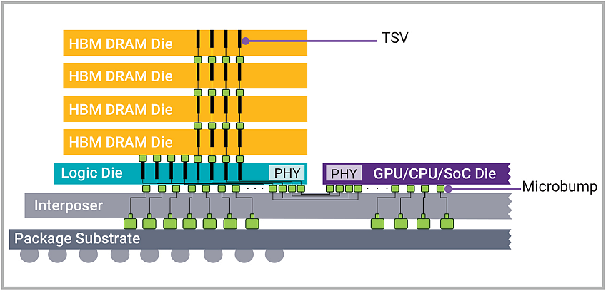
To achieve higher data rates, you can either increase the data rate or the width of the bus. DDR5, LPDDR5, and GDDR all take the approach of ramping up the data rate, which causes signal integrity issues as the time for each bit to transfer across the bus shrinks. HBM, however, uses the “go wider” approach, employing a data bus that is 1024 bits wide. In order to accommodate such a wide bus, HBM-based designs employ a 2.5D interposer to connect the host to the DRAMs, which is effectively a miniature PCB that goes inside the package, as shown in the image below.

HBM provides a high-speed memory interface for 3D stacked synchronous dynamic random-access memory (SDRAM). Soon after commercial HBM memory chips were made available, in early 2013, JEDEC released HBM as an industry standard later that year. The latest step in the evolution is HBM3, which is currently under discussion by JEDEC and could be released as a standard as early as late this year.

In this article, which was originally published on the “From Silicon to Software” blog, we’ll take a closer look at what’s driving the demand for HBM3 and how you can continue to feed our world’s growing appetite for bandwidth.

Architected for High Bandwidth and Low Power

IDC predicts that by 2025, worldwide data will grow to 175 zettabytes, representing a 61% compounded annual growth rate from 33 zettabytes in 2018. Three key locations in this datasphere are traditional and cloud-based data centers, followed by the edge (such as cell towers and branch offices), followed by endpoints (such as IoT devices and smartphones). Through vertical stacking of memory chips and by connecting to the host SoC via 2.5D interposer technology, HBM technology shortens the length in which data must travel, supporting smaller form factors. Its 1024-bit memory bus is significantly wider than that of other DRAM types.

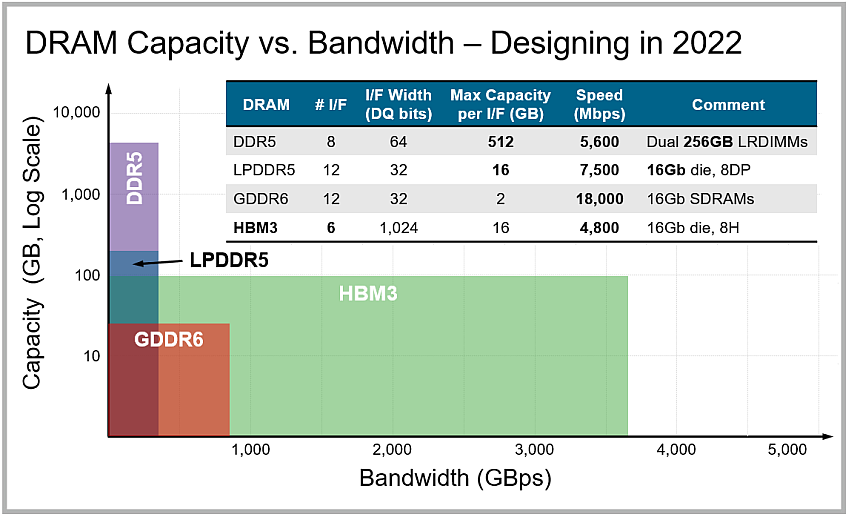
With their high bandwidth and low power consumption owing to shorter, unterminated signals, these interfaces are well-suited for graphics cards, as well as server, high-performance computing (HPC), networking, and high-end AI and machine-learning applications. (The hyperscale data centers that are garnering much buzz these days are driven more by the need for expanding capacity, so their memory type of choice is DDR5.) The graph below highlights the differences in DRAM capacity and bandwidth among different memory types.

HBM brings 3D content into 2.5D designs, which typically consist of a GPU or host SoC and multiple HBM “stacks” assembled side-by-side on an interposer in a single package. Such designs have been an AI workhorse for almost a decade now and are finding their way into market segments such as 5G infrastructure, data centers, and large networking systems. The HBM2E standard enables 8- and 16-GB capacities, with 3.6-Gbps transfer rates and 461-GBps total bandwidth.

The stacked architecture of HBM3 will drive 3DICs for data-intensive applications, providing a way to alleviate the challenges of reticle, die size, and interposer limits. Speculation on what HBM3 will deliver yields these specs:

    • Bandwidth up to 819 GBps
    • Capacity up to 64 GB per stack (as specified by the JEDEC standard, though expect less for real products)
    • 6400-Gbps transfer rates
    • More dies per stack and more than 2x the density per die with a similar power budget
    • The lowest power efficiency of any off-chip DRAM owing to short, unterminated channels.

Although HBM3 has not yet been standardized, some in the industry have already announced designs featuring the super-fast memory. For example, SK hynix has discussed its HBM3 technology that’s in development, noting that it “will be capable of processing more than 665GB of data per second at 5.2 Gbps in I/O speed.”

Unique HBM Design Considerations

Based on its stacked architecture, designing with HBM comes with some unique challenges, the interposer being one of the most notable. An electrical signal conduit, the silicon interposer connects the stacked SDRAM to the processor. There are many design rules around the interposer, which must be custom developed for each chip. The component also adds to the expense of the design.

Logic and DRAM dies are fabricated separately. As part of the HBM flow, through-silicon vias (TSVs), providing the vertical interconnects for the interposers, are formed in each DRAM die, and their uniformity is critical. Microbumps formed on top of the die to provide electrical connections between the different dies create additional challenges related to these fine-pitch structures.

Another HBM design consideration is the limited number of SDRAMs to connect to. With SoCs becoming more complex, especially at advanced nodes, there may only be room for 4-6 HBM stacks as the interposer reaches reticle limits. Once such a chip is built, there’s no flexibility in changing its design down the road, so this should be accounted for at the start of the process. Heat dissipation, too, is an important challenge since DRAMs lose their storage bits faster to leakage at higher temperature.  That can be addressed via lidless packaging technology that allows the heatsink to contact the silicon directly.

Solving Bandwidth Bottlenecks

With the runway to HBM3 shortening as we head to the end of 2021, it’s a good time to make sure that you have in place what you’ll need to keep feeding the hunger for bandwidth. Memory interface IP can help you achieve your memory throughput requirements with minimal power consumption and low latency, while reducing integration risks. Verification IP aligned to the latest protocols helps accelerate runtime, debug, and coverage closure for your designs.

As we continue our efforts to stay ahead of emerging standards, Synopsys has recently announced the industry’s first complete HBM3 IP solution, including controller, PHY, and verification IP for 2.5D multi-die package systems. Synopsys DesignWare® HBM3 Controller and PHY IP, built on silicon-proven HBM3E IP, tap into our interposer expertise to provide a low-risk solution supporting high memory bandwidth up to 921 GBps.

On the verification side, our offerings include our Verification IP with built-in coverage and verification plans, as well as off-the-shelf HBM3 memory models for Synopsys ZeBu® emulation and HAPS® prototyping systems. Additionally, Synopsys 3DIC Compiler multi-die design platform accelerates development of HBM3 system designs through fully integrated architectural exploration, implementation, and system-level analysis.

In a recent news release about our new HBM3 offerings, Cheol Kyu Park, vice president, HBM product champion, and head of DRAM product engineering at SK hynix, noted, “We will leverage our long-standing relationship with Synopsys to provide our mutual customers with fully-tested and interoperable HBM3 solutions that can maximize memory performance, capacity and throughput.”

Memory bandwidth doesn’t have to become a bottleneck. HBM continues evolving to provide a reliable way to quickly move data between a system’s processor and its memory. Once HBM3 becomes standardized, the protocol promises to bring even faster speeds and lower power consumption to our most compute-intense applications.