Nova to acquire ancosys GmbH for $100 million

Nova has entered into a definitive agreement to acquire ancosys GmbH in an all-cash transaction valued at approximately $100 million, including a performance-based earnout of $10 million. The acquisition is expected to close within the first quarter of 2022. ancosys provides chemical analysis and metrology solutions for semiconductor manufacturing. Based in Rehovot, Isreal, Nova provides X-ray and optical metrology solutions for semiconductor’s advanced process control. Among its costumers: TSMC, GlobalFoundries, Micron, Samsung, Hynix and Huali.

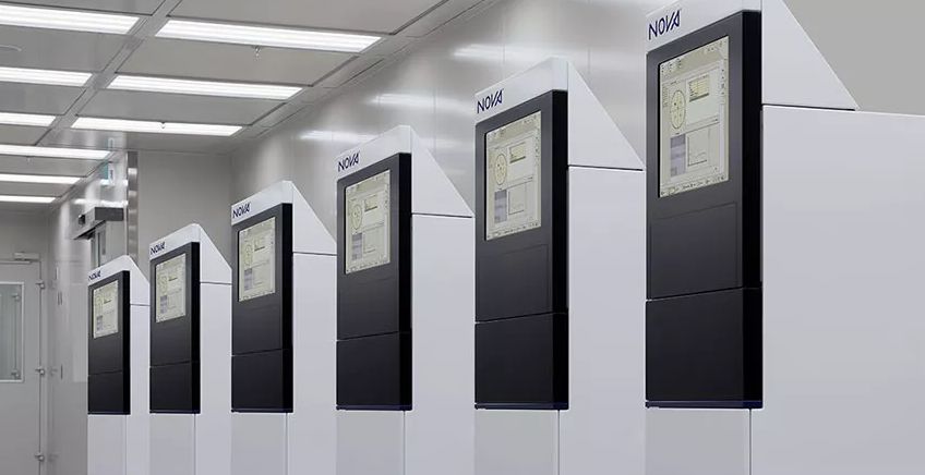
“Acquiring ancosys will support our long-term strategy to broaden our portfolio of key technologies for a wider range of process control applications in different semiconductor markets,” said Eitan Oppenhaim (photo above), President and CEO of Nova. Based in Pliezhausen, Germany, ancosys provides modular systems to measure physical, chemical, and electrochemical properties of materials, based on its open architecture.

According to Oppenhaim, “The next-generation devices require a better approach to control different materials’ properties, along with the ambitious architectural design”. Lately, Nova reported record quarterly revenue of $112.7 million, up 62% compared with Q3 2020. “We now forecast the company revenue for the year to surpass $412 million in revenues. This forecast indicates growth of more than 50% year-over-year.”

University Program Nurtures Next Generation of Engineers

By Patrick Haspel, Global Program Director, Academic Partnerships and University Programs, Synopsys

The COVID-19 pandemic has accelerated our digital migration, moving more of our activities online. Ajit Manocha, president and CEO of SEMI, has discussed how critical it will be for the industry to close the talent gap. Investing in science, technology, engineering, and math (STEM) education is one way to nurture the interests and skillsets that are needed to bring more engineers into the workforce.

Collaborative business/university relationships, where businesses provide resources that complement or augment educational programs, provide a nice bridge between the two worlds. One such example is the Synopsys Electronic Design University Program, which provides academic and research institutions with access to electronic design automation (EDA) software, technical support, curriculum, and more.

The university bundle consists of more than 200 tools for a nominal fee and licensing agreement in support of fundamental research and education efforts. In this article, which was originally published on the From Silicon to Software blog, I’ll highlight some key examples that illustrate the mutually beneficial outcomes that are resulting from close collaboration between the business and academic worlds.

VLSI Training Course at Tel Aviv University

Creating the next generation of chip design engineers needs to start at the university level. Consider a project involving a complex 5nm design, which would require a team for implementation, verification, software design, and more. Such an endeavor could involve more than 100 people who have the latest skills. However, it’s not always easy to find the right mix of engineers.

Israel, for example, is in a region of the world where the dearth of electronic design talent is extremely high. To help create a pipeline of engineers, Zvi Webb, a retired applications engineering director from Synopsys, is serving as VLSI lab manager at Tel Aviv University and is developing an introductory very large-scale integration (VLSI) course based on the latest chip design tools. Students there, Webb noted, hadn’t been exposed to a digital design workflow and tool chain. Instead, they were building their designs manually.

Webb’s course will be offered in the spring of 2022 and will cover topics such as Verilog, logic synthesis, static timing analysis, and placement and routing, providing students with real-world expertise that can help open doors once they’re ready for the workforce. The training outline was derived from material prepared by Professor Adam Teman from Bar Ilan University. “The new course will bring student engineers more knowledge – they will gain an understanding of what VLSI means, what the steps are, how to perform checks,” Webb said.

NC State University Creates PDK for Physical Verification at 3nm

What constitutes an effective 3nm node? According to research conducted by the Electrical & Computer Engineering Department at North Carolina State University, which based its examinations on several IMEC papers, the 3nm node is marked by a gate length of approximately 15nm, cell track height of 5.5T, and contacted poly pitch of 42nm. Scaling has been enabled by design technology co-optimization to achieve the desired benefits; however, as Moore’s Law slows down, it’s now also important to look at system technology co-optimization, examining ways to reengineer the power grid and utilize new device structures (such as gate all-around FETs).

Dr. Rhett Davis, a professor at the university’s Electrical & Computer Engineering Department, has teamed up with graduate students, other faculty, and the Synopsys University Program to create an open-source 3nm process design kit (PDK) for education and industry research. Specifically, the team wanted to explore the impact of new structures like gate all-around FETs and scaling boosters like buried power rails and 5.5T height metal pitch.

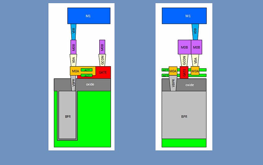
A cross-section of a single transistor in the FreePDK3's vision of a 3nm process (front and side views)
A cross-section of a single transistor in the FreePDK3’s vision of a 3nm process (front and side views)

“What we found when making this kit is that transistors aren’t really shrinking anymore. Instead, they’re getting taller. That is, foundries are finding economical ways to stack them. Our kit compiles the best available public data into a set of rules that show us how to work with this new technology,” explained Davis.

To create the resulting FreePDK3, the team used Synopsys IC Validator for physical verification, Synopsys Custom Compiler for layout and schematic entry, Synopsys StarRC for parasitic extraction, and HSPICE® technology for circuit simulation. The FreePDK3 is published on the GitHub repository.

Engaging the Next Generation of Engineers

These examples illustrate the work that academia is engaging in with the business world. Through our Electronic Design University Program, Synopsys provides full-semester coursework for undergraduate and graduate programs in IC design and EDA development; teaching resources such as libraries and PDKs, and technical support and training. In addition, Synopsys also offers academic programs in the areas of optical design and static analysis software.

The Synopsys Foundation is committed to advancing STEM education opportunities that contribute to the growth and development of our future technology leaders. Through close collaboration, businesses and universities can help nurture the next generation of engineers for semiconductor and electronics industries that are continuing to embark on new innovations that are fueling our smart, connected world.

China-Taiwan Conflict May develop into a Chip-war

US Navy ships sail in formation with Japanese, Australian and Canadian ships in the Philippine Sea. Credit: US DoD

The growing tension between China and Taiwan in the last months raises fears of a coming war and possible takeover of Taiwan’s semiconductor’s capacity, which may reshape the Global Semiconductor Industry. With small population of 24 million people, Taiwan is one of the most important hubs of the semiconductor supply chain. According to IC Insights, in 2020 Taiwan held the largest share of IC industry capacity of any country or region in the world.

Led by TSMC, Taiwan by far holds the largest share of leading-edge (small nodes of less than 10nm) IC capacity (63%) of any country in the world. South Korea, represented by Samsung, holds the remaining 37%. Taiwan holds 22% of the world’s 300mm IC capacity, second only to South Korea, which holds a 25% share.  North America possesses only an 11% share of global 300mm IC capacity. ICs are all semiconductor devices, excluding computer processors.

Taiwan is a Global powerhouse of foundry services: About 80% of Taiwan’s total IC capacity is dedicated to foundry production. Taiwan’s pure-play foundries (TSMC, UMC, Powerchip, Vanguard, etc.) are forecast to represent almost 80% of the total worldwide pure-play foundry market in 2021.

37% of Global IC capacity

A special report by IC Insights, suggests that China is determined to take hold of the Taiwanese semiconductors assets. “If combined, the share of IC capacity within the borders of China and Taiwan would represent about 37% of global IC capacity, about 3x the amount of IC capacity located in North America.”

IC Insights analysts believe that the US sanctions, especially with regard to IC technology, caused China to question how it will be able compete in the future IC and electronics industries.  “It is increasingly apparent that China’s answer to that question centers on its reunification with Taiwan. Currently, there is no more important base of IC capacity and production than Taiwan. China has a huge problem with its inability to produce leading-edge IC devices —a problem that it believes can be solved through reunification with Taiwan by whatever means necessary.

Short term Pain, Long term Gain

What will be the price of a possible war? “While the Taiwanese economy would crater if China attempted a military takeover of the island nation, China’s economy would also suffer greatly.  The question is whether China is willing to accept relatively short-term economic pain for the long term benefit of having the largest amount of the world’s leading-edge IC production capacity under its control for many years to come.”

It is important to mention that IC Insights does not bring evidence to support this conclusion. It also does not mention the deterrent effect of the US forces in the Pacific (photo above). Maybe it is more a warning than a prediction. However, it expresses a real concerns that geopolitical tension in the Taiwan Strait may develop, any moment, into a huge disruption of the entire Global semiconductor supply chain.

NeuroBlade Raises $83 Million in Series B Funding to Accelerate Data Analytics

NeuroBlade, the next generation of data acceleration solutions, announced today that it has secured $83 million in Series B funding, bringing total invested capital to $110 million. The investment was led by Corner Ventures with contribution from Intel Capital, and supported by current investors StageOne Ventures, Grove Ventures and Marius Nacht. Additionally, technology companies including MediaTek, Pegatron, PSMC, UMC and Marubeni also provided funding during this round. The financing will be put to work as the company expands its engineering teams in Tel Aviv and builds out its sales and marketing teams globally.

NeuroBlade has developed a new data analytics architecture that eliminates major data movement bottlenecks by integrating the data processing function inside memory, better known as processing-in-memory (PIM). PIM has been a pipe dream for decades, and according to NeuroBlade, it is the first company to successfully bring this innovation to production. NeuroBlade accelerates data analytics and unclogs traditional bottlenecks by integrating its technology into a full system-level easy-to-deploy appliance.

With more than 100 employees and growing, NeuroBlade has begun shipping its data accelerator to leading-edge customers and partners worldwide. This has seen these partners starting to integrate and deploy NeuroBlade into the world’s biggest data centers.

“We invented a new building block in computer architecture so organizations can quickly answer critical problems facing society and vastly improve business opportunities,” said Elad Sity, CEO and co-founder of NeuroBlade. “Our team is at the core of this success. Together, we built a data analytics accelerator that speeds up processing and analyzing data over 100 times faster than existing systems. Based on our patented XRAM technology, we provide a radically improved end-to-end system for the data center.”

Existing system architectures show that the constant shuffling of data between storage, memory, and central processing is the primary cause of poor application performance and slow response times. NeuroBlade recognized that current architectures cannot scale to meet future data analytics needs, which led them to build a computational architecture that eliminates the data movement requirements and massively speeds data analytics performance.

“Despite being tested like never before this past year, the data center kept the world operating at a critical time. We think that this market is poised for explosive growth and NeuroBlade looks to have a promising journey ahead,” said Lance Weaver, vice president and general manager of Data Center & Cloud Strategy at Intel. “Intel is proud to power NeuroBlade’s platform with our portfolio of products. We look forward to our continued collaboration with NeuroBlade to optimize end-to-end performance.”

“SAP looks forward to continuing to work with NeuroBlade on their new PIM-based data analytics acceleration solution,” said Dr. Patrick Jahnke, head of the innovation office at SAP. “The performance projections and breadth of use cases prove great potential for significantly increased performance improvements for DBMS at higher energy efficiency and reduced total-cost of ownership on-premises and in the cloud. Through this exciting collaboration with NeuroBlade, SAP will unlock new possibilities to build the data center of the future.”

“Organizations run at the speed of their data. NeuroBlade is here to alter the pace of the race. Such is the impact that this technology will have on the global data center market. We fully expect NeuroBlade to be a major player in a very short time and why we are excited to join them at this critical moment in their growth,” said Corner Ventures partner Jonathan Pulitzer.

“In an increasingly digitized world, data empowers businesses to make more informed and precise decisions than ever before,” said Roi Bar-Kat, Head of Intel Capital Israel. “With NeuroBlade’s scalable solution, organizations are better equipped to quickly extract insights needed to make key decisions. Intel Capital is looking forward to supporting the NeuroBlade team as they work to bring increased efficiency and scale to data processing.”

Optimizing PPA for 3DICs Requires a New Approach

By Raja Tabet, Sr. VP of Engineering, and Anand Thiruvengadam, Product Marketing Director, Custom Design and Physical Verification Group

Sponsored by Synopsys.

The adoption of 3DIC architectures is enjoying a surge in popularity as product developers look to their inherent advantages in performance, cost, and the ability to combine heterogeneous technologies and nodes into a single package. As designers struggle to find ways to scale with complexity and density limitations of traditional flat IC architectures, 3D integration offers an opportunity to continue functional diversity and performance improvements, while meeting form-factor constraints and cost.

3D structures offer a variety of specific benefits. For example, performance is often dominated by the time and power needed to access memory. With 3D integration, memory and logic can be integrated into a single 3D stack. This approach dramatically increases the width of memory busses through fine-pitch interconnects, while decreasing the propagation delay through the shorter interconnect line. Such connections can lead to memory access bandwidth of tens of Tbps for 3D designs, as compared with hundreds of Gbps bandwidth in leading 2D designs.

From a cost perspective, a large system with different parts has various sweet spots in terms of silicon implementation. Rather than having the entire chip at the most complex and/or expensive technology node, heterogeneous integration allows the use of the ‘right’ node for different parts of the system, e.g., advanced/expensive nodes for only the critical parts of the system and less expensive nodes for the less critical parts.

In this post, which was originally published on the “From Silicon to Software” blog, we’ll look at 3DIC’s ability to leverage designs from heterogenous nodes– and the opportunities and challenges of a single 3D design approach to achieve optimal Power, Performance, and Area (PPA).

Vertical Dimension Changes the Design Strategy

While 3D architectures elevate workflow efficiency and efficacy, 3DIC design does introduce new challenges. Because of the distinct physical characteristics of 3D design and stacking, traditional tools and methodologies are not sufficient to solve these limitations and require a more integrated approach. In addition, there is a need to look at the system in a much more holistic way, compared to a typical flat 2D design. Simply thinking about stacking 2D chips on top of each other is insufficient in dealing with the issues related to true 3D design and packaging.

Since the designs must be considered in three dimensions, as opposed to the typical x, y aspects of a flat 2D design, everything must be managed with the addition of the z dimension  – from architectural design to logic verification and route connection – including bumps and through-silicon vias (TSVs), thermal, and power delivery network (PDN) opportunities for new tradeoffs (such as interposer based versus 3D stacks, memory on logic or logic on memory, and hybrid bonding versus bumps). Optimization of the ‘holy grail’ of PPA is still a critical guiding factor; however, with 3DICs, it now becomes cubic millimeter optimization, because it’s not just in two directions, but also the vertical dimension that must be considered in all tradeoff decisions.

The need for Co-design Methodology

Further complicating matters, higher levels of integration available with 3DICs obsolete traditional board and package manual-level techniques such as bump layout and custom layout for high-speed interconnects, which cause additional bottlenecks. Most importantly, interdependency of previously distinct disciplines now needs to be considered in a co-design methodology (both people and tools), across all stages of chip design, package, architecture, implementation, and system analysis.

Let’s look at an example of a specific design challenge – the goal to improve memory bandwidth. Traditionally, designers would look at how to connect the memory and CPU to get the highest possible bandwidth. But with 3DICs, they need to look at both the memory and CPU together to figure out the optimal placement in the physical hierarchy, as well as how they connect, through CSVs or silicon vias, for example. While performance is critical, designers need a way to evaluate the power and thermal impact by stacking these types of elements together in different ways, introducing new levels of complexities and design options.

Taking a Silicon-First Approach

While it might seem obvious to consider a 3D architecture in a similar manner as a printed circuit board (PCB) design, 3DICs should ideally take a silicon-first approach – that is, optimize the design IP (of the entire silicon) and co-design this silicon system with the package. Within our approach to 3DICs, Synopsys is bringing key concepts and innovations of IC design into the 3DIC space. This includes looking at aspects of 3DICs such as architectural design, bringing high levels of automation to manual tasks, scaling the solution to embrace the high levels of integration from advanced packaging, and integrating signoff analysis into the design flow.

3DICs integrate the package, traditionally managed by PCB-like tools, with the chip. PCB tools  are not wired to deal with both the scale complexity and process complexity. In a typical PCB there may be 10,000 connections. But in a complex 3DIC, there are hundreds of millions of connections, introducing a whole new level of scale which is far outpacing what older, PCB-centric approaches can manage. Existing PCB tools cannot offer assistance for stacking dies, and there is no package or PCB involved. Further, PCB tools cannot look at RTL or system design decisions.

The reality is that there cannot be one single design tool for all aspects of a 3DIC (IC, interposer, package), yet there is an acute need for assembling and visualizing the complete stack. The Synopsys 3DIC Compiler does just that. It is a platform that has been built for 3DIC system integration and optimization. The solution focuses on multi-chip systems, such as chip-on-silicon interposer (2.5D), chip-on-wafer, wafer-on-wafer, chip-on-chip, and 3D SoC.

The PPA Trifecta

Typically, when you think of large complex chips, the first optimization considered is area.  SoC designers want to integrate as much functionality into the chip and deliver as high performance as possible. But then there are always the required power and thermal envelopes, particularly critical in applications such as mobile and IoT (and also high-performance computing). Implementing 3D structures enables designers to continue to add functionality to the product, without exceeding the area constraints and, at the same time, lowering silicon costs.

But a point tool approach only addresses sub-sections of the complex challenges in designing 3DICs. This creates large design feedback loops that don’t allow for convergence to an optimal solution for the best PPA per cubic mm2 in a timely manner. In a multi-die environment, the full system must be analyzed and optimized together. It isn’t enough to perform power and thermal analysis of the individual die in isolation. A more effective and efficient solution would be a unified platform that integrates system-level signal, power, and thermal analysis into a single, tightly coupled solution.

This is where 3DIC Compiler really shines–by enabling early analysis with a suite of integrated capabilities for power and thermal analysis. The solution reduces the number of iterations through its full set of automated features while providing power integrity, thermal, and noise-aware optimization. This helps designers to better understand the performance of the system and facilitate exploration around the system architecture.  And it also allows a more efficient way to understand how to stitch together various elements of the design and even connect design engineers in some ways to traditional 2D design techniques.

Ideal Platform for Achieving Optimal PPA Per Cubic mm2

Through the vertical stacking of silicon wafers into a single packaged device, 3DICs are proving their potential as a means to deliver the performance, power, and footprint required to continue to scale Moore’s law. Despite the new nuances of designing 3D architectures using an integrated design platform, the possibilities of achieving the highest performance at the lowest achievable power makes 3D architecture appealing. 3DICs are poised to become even more widespread as chip designers strive to achieve the optimum PPA per cubic mm2.

Newsight and ZKW to develop smart light beams

Above: Newsight and ZKW’s Smart lighting module on a test wehicle

The Israeli startup Newsight Imaging and the Austrian based ZKW Group have completed the development of a new prototype of a car’s smart glare-free high beam that can be integrated directly into the headlamp with its associated sensors and controller. This eliminates the need for a separate front camera. The project, which is currently known as “senseZ” could be ready for series production soon and be manufactured by ZKW.

“The autonomous high beam system can be added to or used to retrofit older vehicle models that do not have a front camera or an infrastructure designed for ADB. It can also be used to upgrade existing adaptive high beam technology with a higher resolution,” said Oliver Schubert, CEO of ZKW Group. The innovation is easy to integrate into the vehicle architecture, because neither the vehicle electronics nor camera data from the vehicle itself are required.

The new system consists of an integrated module for glare-free high beams which is installed in the headlamp. The control signals for the adaptive light are delivered by a light-sensitive sensor that is also integrated into this “senseZ” unit. This allows for intelligent, vehicle-independent control of the high beam that automatically hides other road users at night, actively helping to improve traffic safety. An initial prototype in a test vehicle (Audi A1) will now be used to optimize the unit’s function. “Now, we are taking the next step together through further development and joint commercialization,” says Hannes Scheer, Head of Innovation at ZKW Group.

Newsight Imaging Ltd. (www.nstimg.com) develops CMOS image sensor chips, providing 3D solutions for high volume markets, replacing more expensive CCD sensors and other camera modules in LiDAR applications for robotics, automotive and more. Headquartered in Wieselburg, Austria, ZKW Group designs and produces complex premium lighting and electronic modules for international automakers such as Audi, BMW, Daimler, VW, Volvo and more.

Memory, auto-specific, and MPUs to drive Semiconductors growth

Imec Semiconductors Technology

Computing has long been the growth engine for the IC industry*, but remarkable emerging applications in communication, consumer, automotive, and industrial/medical systems are fueling development of new complex, high-speed, and/or low-power ICs.  Cloud computing, 5G technology, artificial intelligence, virtual reality, the Internet of Things, autonomous vehicles, robotics, and many other technologies are rapidly advancing and will change the way consumers live and businesses operate.

According to IC Insights, a strong, we are facing athree-year wave of double-digit growth for the IC industry based on these emerging technologies. Electronic system sales are forecast to rise 8% while the 2021 IC market is forecast to rise 12% and set a new all-time high sales level of $441.5 billion, which would surpass the previous high mark of $421.7 billion set in 2018.  A big 15% surge in semiconductor industry capital spending is forecast for this year as TSMC and Samsung are moving to expand their respective 7nm and 5nm manufacturing capacity.  TSMC also expects to ramp production of 3nm devices by the end of the year.

The researchers identified 10 top-growing IC product categories is expected to see a double-digit increase in sales, but only the top-five segments of them are forecast to grow faster than the total IC market (12% this year). DRAM and NAND flash are expected to be the two fastest-growing product segments in 2021 with 18% and 17% sales growth, respectively.  DRAM was also ranked as the fastest-growing IC segment in 2013, 2014, 2017, and 2018.  On the other hand, due to its extreme cyclicality, DRAM has also been among the poorest performing categories in 2019 when collapsing prices resulted in the DRAM market fall of -37%.

An increase in laptop, tablet, and server system sales boosted NAND revenue 24% in 2020 as the Covid-19 pandemic forced a transformation in the way consumers, schools, businesses, and governments communicated and carried on with their business.  The transition to 5G technology within many of these same computing applications and smartphones is forecast to boost NAND revenue growth 17% in 2021.

Two automotive specific IC product categories, Automotive—Application-Specific Analog and Automotive—Special Purpose Logic are forecast to be among the fastest growing segments in 2021. New car sales took a hit during Covid-plagued 2020, which adversely impacted automotive IC sales. But demand for automobiles picked up in early 2021, leading to shortages of many automotive IC products.  Additional electronic systems/features, onboard connectivity, advances in autonomous driving, and the expansion of electronic vehicle sales around the world are expected to help raise the average semiconductor content per new vehicle to more than $550 in 2021.

With smartphone growth slowing in recent years, many system-on-chip MPU suppliers such as Qualcomm, Samsung, and MediaTek, have turned more of their attention to 64-bit embedded processors that integrate security features and machine-learning AI acceleration along with graphics and video capabilities for automated vehicles, self-flying drones, and IoT applications.  In a growing number of applications, embedded processors are handling machine-learning AI capabilities for autonomous operations without the need of intervention or control by humans.

The 32-bit MCU market has expanded rapidly because of increasing demands for higher levels of precision in embedded systems and the rush to the Internet of Things. Many new 32-bit MCU designs support wireless connections and Internet protocol (IP) communications. In automobiles, 32-bit MCU demand is being driven by “intelligent” onboard systems and increases in real-time sensor functions.  Meanwhile, a growing wave of 32-bit microcontrollers are being used in a wide range of consumer and industrial equipment applications. This is also driven by the fact that the cost new powerful MCUs is nearly the same as 8-bit and 16-bit devices.

*IC industry covers all the semiconductors products beside computer’s microprocessors.