Zebra Medical Vision from Kibbutz Shefayim near Tel Aviv completed a $30M in C round funding, bringing the total investment in the company to $50M. The company also company is unveiled its latest product: A comprehensive AI Chest X-Ray Reader. The investment round was led by aMoon Ventures with the participation of strategic healthcare investors Aurum, Johnson & Johnson Innovation JJDC Inc. and Intermountain Healthcare and leading global AI scientists Professor Fei Fei Lee and Richard Socher. These new investors are joining a list of existing investors Khosla Ventures, NVIDIA, Marc Benioff, OurCrowd and Dolby Ventures who also participated in this C round.
The chest x-ray AI analytics product was trained using nearly 2 million images to identify 40 different common clinical findings. The results of the study (Textray chest x-rayresearch) establish a new bar for AI research in medical imaging, demonstrating high rates of agreement between the algorithm and human radiologist experts. This publication continues Zebra-Med’s mission to drive a higher standard of care across the radiology domain and collaborate with the medical community to improve patient care.
Zebra Medical Vision uses deep learning to create its Imaging Analytics Platform. The Company was founded in 2014 by Eyal Toledano, Eyal Gura, and Elad Benjamin and funded by Khosla Ventures, Marc Benioff, Intermountain Investment Fund, OurCrowd and Dolby Ventures. It has received the CE regulatory mark for seven of its products, and continues to build a strong pipeline of AI based products. It’s most recent announcements were the CE approval of CT brain bleed and mammography lesion detection algorithms. On its path to build the world’s most comprehensive visual lab, the company’s current and future arsenal of AI algorithms is bundled into a unique $1 per scan offering to hospitals, in order to meet the vision of scalable and affordable care globally.
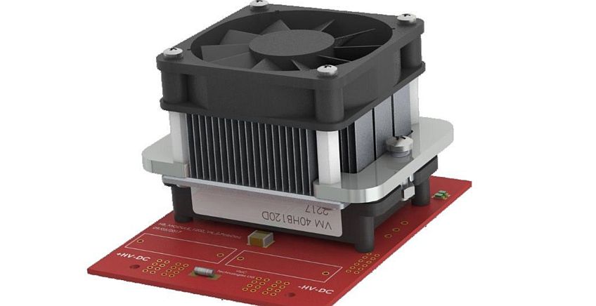
VisIC Technologies from Nes Ziona, Israel, announced today that it has closed $10 million in a Series D round of financing led by a private investor. “With the new funding, we can expand our portfolio further to address more market segments,” said Tamara Baksht, VisIC Technologies’ co-founder and CEO. VisIC was established in 2010 by experts in Gallium Nitride (GaN) technology to develop and sell advanced GaN-based power conversion products.
Last February it started sampling the industry’s first 1200V GaN modules, and announced a major manufacturing partnership with TSMC on their GaN on silicon technologies that were announced in 2017. The company’s 1200V module, based on TSMC’s 650D GaN-on-Silicon process, provides switching time below 10 nanoseconds is ensured by a high electron mobility transistor (HEMT) design, where electrons flow in a 2-dimentional quantum well, which fundamentally differs from electron flow in SiC MOSFETs.
This GaN module offers typical on resistance of just 40 mΩ. Target applications are power converters for motor drives, three-phase power supplies and other applications requiring current switching up to 50 A. “GaN has better fundamental physical properties, such as maximal breakdown field and current density, than those of silicon or SiC,” said VisIC CTO Gregory Bunin.”The manufacturing partnership with TSMC allows VisIC to ramp capacity very quickly.”
According to Occams Business Research, the global GaN power device market is expected to grow with a CAGR of over 24% during the forecast period of 2016-2023. Yole Développement estimates that the GaN power device market is about to reach over US$ 332,5 million in 2022. Gallium Nitride (GaN) is a chemical compound made of gallium and nitrogen. It is considered a wonder material due to its high band gap energy of 3.4 electron volt, compared to 1.14ev in silicon and 0.67ev in germanium. The high band gap energy of the gallium nitride made it ideal to use in power electronics industry.
Photo above: VisIC Technologies’ power GaN module with external cooling system
In radar applications, phase noise is a critical performance metric for systems requiring high clutter attenuation. Phase noise is a concern for all radio systems, but radar in particular can require phase noise performance at frequency offsets much closer to the carrier than a communication system.
System designers in these high performance systems will choose ultra low phase noise oscillators and the objective of the signal chains, from a noise perspective, is to add minimal degradation to the oscillator phase noise profile. This requires residual or additive phase noise measurements of the varied components in the signal chain.
Recent product releases of high speed digital-to-analog converters (DACs) are extremely attractive for both waveform generation and frequency creation for any LOs needed in frequency conversion stages. The radar objectives, however, challenge the DAC phase noise performance.
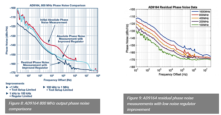
In this article, we show measured improvements of over 10 dB at 10 kHz offsets using the AD9164 DAC. Figure 1 illustrates the improvement and we will discuss how the results were achieved through a combination of both power supply regulator selection and test setup improvements.
Phase Noise Definition
Phase noise is a measure of the deviation in the zero crossing of a periodic signal. Consider a cosine wave with phase fluctuations:
Phase noise is determined from the power spectral density of the phase variations:
In linear terms, the single sided phase noise is defined as:
Phase noise is normally expressed in units of dBc/Hz from 10log(L(f)). Phase noise data is then plotted at offset frequencies relative to the RF carrier.
An important further definition of phase noise is absolute phase noise vs. residual phase noise. Absolute phase noise is the total phase noise measured in the system. Residual phase noise is the additive phase noise of the device under test. This distinction becomes critical in the test setups and in the process of determining component level phase noise contributions in a system.
DAC/DDS Phase Noise Measurement Methods
The figures in this section illustrate DDS phase noise test setups. For DAC phase noise measurements, it is assumed the DAC is used as part of a direct digital synthesizer (DDS) subsystem. A DDS is implemented with a digital sinewave pattern to a DAC that could be in a monolithic IC or an FPGA or ASIC communicating to a DAC. In modern DDS design, the digital phase errors can be made much less than the DAC errors, and DDS phase noise measurements are typically limited by the DAC performance.
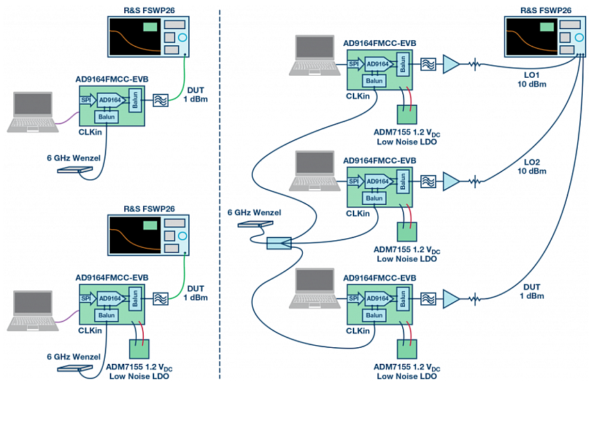
The simplest and most common test setup is shown in Figure 3. A clock source is used for the DDS and the DDS output is fed to a cross correlation type phase noise analyzer. This is easy to implement since only a single DDS is required. However, with this test setup, there is no method to extract the oscillator contribution to show only the DDS phase noise.
Figure 4a shows the phase detector method. In this case, two DACs are used and the oscillator contribution subtracts from both DUTs in the downconversion to dc.
Figure 4 shows two common methods to remove the oscillator phase noise from the measurement, providing a residual noise measurement. The drawback of the measurements is that additional DACs are required in the test setup. However, the benefit is a much better indicator of the DAC phase noise contribution that can be applied in system-level analysis budgets.
Figure 4b shows a method using cross correlation phase noise analysis. In this case, DDS2 and DDS3 are used to translate the clock contribution to the LO ports of the measurement, their contribution is removed in the cross correlation algorithms, and the DDS1 residual phase noise is obtained in the measurement.
Figure 4a: DDS residual phase noise measurement using the phase detector method Figure 4b: DDS residual phase noise measurement using the cross correlation method
Power Supply Noise Contributions
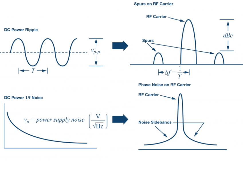
In low noise analog and RF design, power supply noise is a well-known factor to consider. Power supply ripple that is periodic modulates onto the RF carrier and creates spurs on the RF carrier at frequency offsets equal to the ripple frequency. Regulator 1/f noise modulates onto the RF carrier also and contributes to the phase noise profile. Figure 5 illustrates the principles.
Figure 5: Power supply imperfections modulated on to the RF carrier
Measured Results
During investigation of the true DAC phase noise performance, both the test setups and the regulator noise performance were considered.
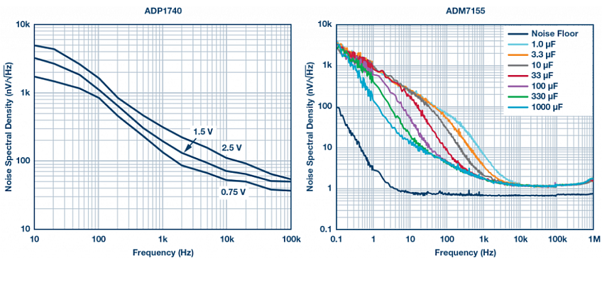
The initial DAC evaluation board included the ADP7140 regulator for the analog and clock voltages. Noise spectral densities were compared with recently released ultra low noise regulators and the ADM7155 was chosen. Figure 6 illustrates the comparison of the noise densities as shown in the product data sheets. The power supply modification was merely to use the ADM7155 for both the AD9164 clock (data sheet pins VDD12_CLK) and the analog voltage (data sheet pins VDD12A).
Figure 6: Regulator noise density comparison. Note the Y-axis units—the ADM7155 is an order of magnitude improved
Next, test setup options were considered for residual phase noise measurements. The cross correlation method was chosen with the Rohde and Schwarz FSWP primarily out of availability and convenience. The test setup used is shown in Figure 7.
Figure 7: Test setups for AD9164 phase noise measurements
Figure 8 is a measurement of three cases. The initial evaluation board measurement taken with an absolute phase noise approach is shown as the red curve. The light blue curve is also an absolute measurement, but with the regulator improvement. The dark blue curve is a residual phase noise measurement that also includes the regulator improvement.
The measurement indicates three general regions of limitations in the initial measurement that were not obvious in the beginning of the investigation. Frequencies below 1 kHz were limited by the close in noise of the clock source. Frequencies from 1 kHz to 100 kHz were limited by the regulator selection. Frequencies above 100 kHz were limited by the clock source. The sharp drop off above 10 MHz is the clock source contribution, as the clock used was a multiplied crystal oscillator to create 6 GHz and the roll-off is from the RF filters used in the multiplication stages.
Residual phase noise measurements with the regulator improvement were taken at additional DAC frequencies and several are summarized in Figure 9. The modifications were duplicated on several evaluation boards and all cases showed the same improved results.
The family of ultra low noise regulators with similar noise density is shown in Table 1. As demonstrated, the impact on the DAC phase noise is significant and these are also recommended for consideration for any areas of the RF system requiring optimum phase noise performance.
Table 1: Family of regulators with state-of-the-art noise density performance. 1 Noise independent at fixed output voltage
Summary
A phase noise review was provided for the fundamental definition, absolute vs. residual phase noise, DAC phase noise measurement test setups, and regulator noise contributions.
DAC phase noise improvements were demonstrated for including both residual phase noise test methods and optimum regulator selection. The end result is the AD9164 now is an enabler for ultra low phase noise, DDS-based applications when the analog voltages and clock voltages are powered from the Analog Devices family of low noise regulators.
References:
Bergeron, Jarrah, “Analyzing and Managing the Impact of Supply Noise and Clock Jitter on High Speed DAC Phase Noise,” Analog Dialogue, Vol. 51, 2017.
Calosso, Claudio E., Yannick Gruson, and Enrico Rubiola, “Phase Noise and Amplitude Noise in DDS,” IEEE Frequency Control Symposium, 2012.
Jayamohan, Umesh, “Powering GSPS or RF Sampling ADCs; Switcher vs LDO,” Analog Dialogue, Vol. 50, 2016.
“Product Note 11729B-1, Phase Noise Characterization of Microwave Oscillators: Phase Detector Method,” Agilent, May, 2007.
Reeder, Rob, “Designing Power Supplies for High Speed ADC,” Analog Devices, Inc., 2012
Walls, Warren F. “Cross Correlation Phase Noise Measurements,” IEEE Frequency Control Symposium, 1992.
Authors
Peter Delos [peter.delos@analog.com] is a technical lead at Analog Devices, Inc., in the Aerospace and Defense Group. Jarrett Liner [ jarret.liner@analog.com] is an RF systems application engineer with Analog Devices, Inc., in the Aerospace and Defense Group in Greensboro, NC.
Applied Materials, Inc. today announced a breakthrough in materials engineering that accelerates chip performance by up to 15%. The company said this is first metal change to transistor contact and interconnect in 20 years after the introduction of copper. “It removes major performance bottleneck at the 7nm foundry node and beyond. Materials such as tungsten and copper are no longer scalable beyond the 10nm foundry node because their electrical performance has reached physical limits for transistor contacts and local interconnects.”
This has created a major bottleneck in achieving the full performance potential of FinFET transistors. “Five years ago, Applied anticipated an inflection in the transistor contact and interconnect, and we began developing an alternative materials solution that could take us beyond the 10nm node,” said Dr. Prabu Raja, senior vice president of Applied’s Semiconductor Products Group. For the 7nm node and beyond, the increasing resistance in tungsten gapfill results in higher power consumption and slower chip performance.
First-level copper interconnects face similar challenges as resistance rises with decreasing copper volume, also slowing chip performance. Cobalt also demonstrates better line and via resistance scaling and less electromigration than copper, facilitating higher current densities. Cobalt is about to remove this bottleneck, but it requires a change in process system strategy. The company combined three new deposition processes are complemented by a new anneal product and a production-proven CMP tool to comprise an end-to-end process suite that makes it possible to use cobalt as a conducting material.
It includes: Applied Endura Cirrus RT PVD Cobalt To deposit the initial thin layer of cobalt to which the subsequent CVD cobalt adheres. Applied Endura Volta CVD Co to deposit the cobalt fill following the PVD layer. The seam created by this deposition process is subsequently eliminated during the anneal step. Applied Endura Versa XT PVD Co to deposit the thick overburden following the anneal step. Applied Producer Pyra Anneal to heats the wafer, causing cobalt reflow that eliminates the seam in the bulk fill, enlarges the grain size, purifies the cobalt, and reduces the resistance. Applied Reflexion LK Prime CMP: Using slurries specifically optimized for polishing cobalt, this system removes the overburden produced by earlier deposition steps and creates a planar surface for subsequent process steps.
Applied’s integrated cobalt suite is now shipping to foundry/logic customers worldwide.
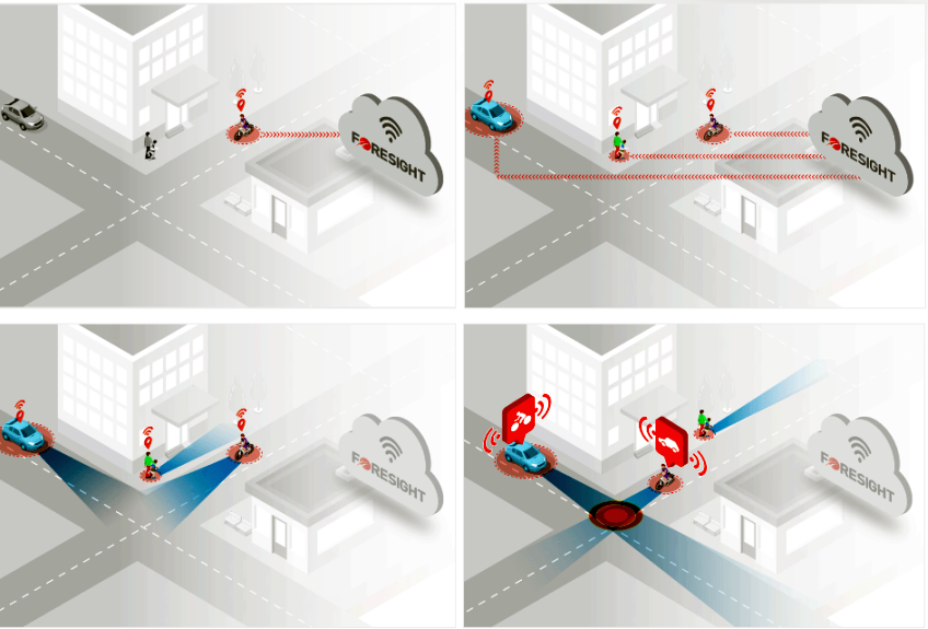
Foresight has successfully completed a controlled trial of its Eye-Net accident prevention solution done in the city of Ashdod, Israel. Eye-Net is a V2X cellular-based accident prevention solution, designed to provide pre-collision alerts in real time to pedestrians and vehicles by using smartphones and relying on existing cellular networks.
The trial was conducted at a central intersection in Ashdod, a city in the center of Israel, and was carried out in collaboration with NoTraffic Ltd., which develops traffic management systems for cities based on a network of sensors deployed at intersections with traffic lights. Supervision was provided by BWR (Blue and White Robotics) as part of the Ashdod Smart Mobility Living Lab project, and the trial was carried out with the support of the Ministry of Transport and the Ayalon Highway company.
In the first part of the trial, several accident-simulated scenarios including vehicles and/or a pedestrian were performed. In all cases, the parties were using the Eye-Net application installed on their cellular phones and received real-time alerts in order to prevent a collision. The second part of the trial tested the integration of Eye-Net with NoTraffic’s smart infrastructure system in accident-simulated scenarios where only one of the vehicles involved was connected to the Eye-Net system. NoTraffic’s system, which was installed at the intersection, identified the non-connected driver or pedestrian using a smart sensor, and transmitted the information to the driver using the Eye-Net system, in order to prevent a collision.
Haim Siboni, CEO of Foresight, said that the integration with the NoTraffic system enabled Foresight to examine a variety of realistic scenarios. “We intend to continue the development process in order to achieve extensive exposure for our company’s unique, life-saving technology.” Tal Kreisler, CEO of NoTraffic, said the trial was a breakthrough in the field of smart transportation. “It presents, for the first time, a collaboration between infrastructure. This is a significant milestone. The scenarios demonstrated in the trial are based on recent fatal accidents of connected and autonomous vehicles.”
How it Works
The Eye-Net V2X (vehicle to everything) cellular-based accident prevention solution is designed to provide real-time pre-collision alerts to pedestrians and vehicles. The phone is aware of its location and constantly transmits it to Eye-Net servers. These servers send the location of other devices in the vicinity to each device, effectively making each device aware of the road users around it. The Eye-Net application constantly searches for potential collisions, and once an oncoming collision is detected, immediate visual and audio alerts are sent out to all users involved.
Xiaomi plans to introduce a smartphone 3D camera based on the structured light technology developed by Mantis Vision from Petah Tikva. The two companies announced a strategic partnership. As part of the collaboration, Xiaomi will integrate a 3D camera, operated by Mantis Vision, as the 3D front camera in the company’s flagship device Mi8, which was announced last week by Xioami at the Augmented World Expo (AWE) in Santa Clara California.
Xiomi’s new Mi8 device is the world’s first Android device with integrated 3D imaging and scanning capabilities. Mantis Vision’s technology will enable these capabilities in Android devices for the first time ever, which will allow to scan face scanning and recognition, face 3D capturing for a secure ePayment and other features that have so far only been available with 2D image analysis software. Moreover, the new technology will enable Augmented Reality features both for end users as well as for developers.
Mantis Vision’s technology is based on a patented structured light and a smart decoding algorithm which produce the many depth points with high quality. Its technology allows a 4mm thickness camera, making it suitable for any form factor, including; mobile, smart connected devices, multi-camera volumetric solutions and professional hand-held scanners. The company says that its coded pattern, yields at least 4 times more critical features density, relative to competitors. The result is a high resolution of 120K points when using 1M sensor, or 40K points when using a VGA Sensor.
According to Gur Arie Bittan, founder and CEO of Mantis Vision: “Shrink optical stack and size from centimeters to millimeters, incorporate Vcel lasers that were still nascent technologies at the time, meet OEM’s power consumption needs and conform with eye safety regulations.”
Lately, Mantis Vision and China Luenmei Quantum Co Ltd, a publicly traded company in Shanghai, recently joined forces and created a Joint Venture named “Tang Lang” which is Mantis Vision exclusive partner for the Greater China market. Tang Lang is located in Beijing and Shanghai.
The Xiaomi Mi8 includes a 6.2in OLED screen (2248×1080) from Samsung, and a Qualcomm Snapdragon 845 processor with 6GB of RAM and 256GB of storage. It employs dual 12Mp rear cameras and a 20Mp front camera that uses Mantis Vision IP to provide 3D Face Unlock, even in dark conditions.
After entering the Israeli market and signing a partnership agreement with Beckermus Technologies Ltd, the Caesaria-based manufacturer of micro-electronics, the Philippine production contractor Integrated Micro-Electronics Inc., is planning to increase its activities in Israel.
In an interview with Techtimes, Carla Buencamino, manager of sales and business development for Asia (not including China and Japan) of the Philippines’ Integrated Micro-Electronics Inc., explained the strategy behind the entry into the Israeli market and how the company came to the conclusion that such a small and remote market is important for its long term strategy.
Why did you decide to work with Israel?
Buencamino: “We have already had some costumers in Israel, but the business volumes remained constant an unchanged, while the local industry grew impressively. The Israeli technology industry precisely represent the type of markets we are looking for: growing and innovative. We started to check how we can play a greater role in the market, and when we realized that a huge amount of Israeli production is going outsourced to China, we understood there is a good opportunity for us in Israel.
” We can supply the Israeli market with production services that will compete the Chinese services. Our proposition is clear: we do not intend to remove production from Israel, but to provide additional alternatives to the same production agreements that are outsourced from Israel.”
What is your added value over Chinese competitors?
“We are a global company and we operate in many regions besides Asia, including in Europe. In addition, we enjoy a very significant government support by means of free-trade zones, which provide us with incentives and tax breaks, very efficient logistic services and workforce costs that are lower than these costs in China. Furthermore, we get very strong financial backing from the Ayala Group, the owner of Integrated Micro-Electronics Inc.”
European production facility operated by Integrated Micro-Electronics Inc.
Why have you signed a partnership agreement with Beckermus?
“We came to the conclusion that Israel has many tech companies that are suitable for us, but they are vary fast moving companies. So we looked for a local partner that will help us provide very agile NPI services. Beckermus provides this service as well as customer support with the transferring of the mass production to Integrated Micro-Electronics Inc. Today we are developing special expertise in growing markets such as optics, vehicle parts, IoT and cameras. Beckermus provides us with micro-electronics capabilities. Perhaps the next center will be in RF. We are interested in synergy with Israel with regard to our main investment areas. And the opportunity is great.”
Targeting the Aerospace Industry
Carla believes there is a match between the company and the Israeli market: “Our future is in cars and autonomous driving. Israel has many technologies for driverless cars and advanced photography. The local companies fulfill key functions in the markets we want to lead. During 2016 we bought a controlling share in the German’s VIA Optronics, which provides complex optic systems production and fabrication and in mid 2017 we purchased the British STI Enterprises, which supplies EMS services to the security industry. These deals make us more attractive to Israeli costumers, specially in the Aerospace markets.”
Integrated Micro-Electronics Inc. is a production powerhouse that competes with Chinese manufacturing contractors. During 2017 it was ranked 18th in the world in terms of sales. It is owned 50% by the Philippines’ Ayala Group and currently employs 15,000 people in 20 production plants in China, the Philippines, United States, Mexico, Bulgaria, Czech Republic, Germany and the United Kingdom. During the first quarter of 2018, sales rose by 38% to $326 million. Within this, sales at VIA doubled to $52 million and sales at STI totaled $26.6 million.
We use cookies to personalize content and ads, to provide social media features and to analyze our traffic. We also share anonymous information about your use of our site with our social media, advertising and analytics partners. View more
What personal data we collect and why we collect it
We collect anonymous data on visitors in this website for business purposes such as enhancing user experience, digital marketing and search engine optimization.
We collect personal data such as email address and names on various forms - all forms present in this website include consent checkboxes and clear reason for collecting the data: general inquiries on our products, newsletter subscription, professional inquiries job applications. All forms are designed in accordance with GDPR requirements.
Comments
When visitors leave comments on the site we collect the data shown in the comments form, and also the visitor’s IP address and browser user agent string to help spam detection.
An anonymized string created from your email address (also called a hash) may be provided to the Gravatar service to see if you are using it. The Gravatar service privacy policy is available here: https://automattic.com/privacy/. After approval of your comment, your profile picture is visible to the public in the context of your comment.
Media
If you upload images to the website, you should avoid uploading images with embedded location data (EXIF GPS) included. Visitors to the website can download and extract any location data from images on the website.
Contact forms and newsletter
We use Gravity Forms as our platform of choice for all forms present in this website. Forms present in this website have been modified to fit GDPR requirements.
Unless specifically specified and approved by visitor, we do not use the collected data for marketing purposes.
We use Mailchimp to collect email addresses and send periodical marketing materials to our customers.
Handling and management of all email addresses and mailing operations is conducted under GDPR terms and guidelines provided by Mailchimp.
All subscribers are able to change their subscriptions preferences or unsubscribe at any given time.
Techtime has accepted the Data Processing Addendum agreement provided by Mailchimp for all its Mailchimp accounts.
All our lead collection forms have been altered in accordance with GDPR requirements and now include unchecked checkboxes in order to accept the explicit consent of the user prior to form submission.
Cookies
If you leave a comment on our site you may opt-in to saving your name, email address and website in cookies. These are for your convenience so that you do not have to fill in your details again when you leave another comment. These cookies will last for one year.
If you have an account and you log in to this site, we will set a temporary cookie to determine if your browser accepts cookies. This cookie contains no personal data and is discarded when you close your browser.
When you log in, we will also set up several cookies to save your login information and your screen display choices. Login cookies last for two days, and screen options cookies last for a year. If you select "Remember Me", your login will persist for two weeks. If you log out of your account, the login cookies will be removed.
If you edit or publish an article, an additional cookie will be saved in your browser. This cookie includes no personal data and simply indicates the post ID of the article you just edited. It expires after 1 day.
Embedded content from other websites
Articles on this site may include embedded content (e.g. videos, images, articles, etc.). Embedded content from other websites behaves in the exact same way as if the visitor has visited the other website.
These websites may collect data about you, use cookies, embed additional third-party tracking, and monitor your interaction with that embedded content, including tracing your interaction with the embedded content if you have an account and are logged in to that website.
Analytics
We use Google Analytics regularly for monitoring user behavior and traffic sources and utilize the gathered information for enhancing user experience and for business purposes.
The use of Google Analytics in done according to GDPR terms and guidelines provided by Google.
Legal Entity: Techtime.
Primary Contact (a.k.a. "Notification Email Address"): roni@techtime.co.il - this email is designated for receiving notices under the Google Ads Data Processing Terms.
Who we share your data with
We use various cloud platforms and third party providers for the purpose of operating this website.
We do not share or sell your data for any commercial purpose other than specified above.
We use the following processors for the operating this website and executing related digital marketing campaigns:
WP Engine - Hosting Provider
Cloudflare - Cloud based security and web performance processor.
Google Cloud Platform - data centers provider for WP Engine
Sucuri - Website security provider
Mailchimp - Newsletter service provider
Google Analytics, Adwords, Webmasters
Facebook - We use Facebook for advertising and place tracking code on our website for enhancing digital marketing campaigns (i.e - Facebook Pixel).
Planwize Ltd - Digital Marketing Agency.
How long we retain your data
If you leave a comment, the comment and its metadata are retained indefinitely. This is so we can recognize and approve any follow-up comments automatically instead of holding them in a moderation queue.
For users that register on our website (if any), we also store the personal information they provide in their user profile. All users can see, edit, or delete their personal information at any time (except they cannot change their username). Website administrators can also see and edit that information.
What rights you have over your data
If you have an account on this site, or have left comments, you can request to receive an exported file of the personal data we hold about you, including any data you have provided to us. You can also request that we anonymize or erase any personal data we hold about you. This does not include any data we are obliged to keep for administrative, legal, or security purposes.
Request for Receiving Data Associated with One’s Email Address
Users may request to receive access to all related information submitted to this website for their review.
In accordance with GDPR compliance, user may further request the anonymization of such data.
In order to request access for all data associated with a given email address, users may submit the request here. Users then receive an email with a link to a page with all related information.
The link is valid for 24 hours. Users may submit additional request for the same email address once in every 24 hours.
A request for anonymization should be sent separately: User may select the data he or she wishes the site owner to anonymize so it cannot be linked to his or her email address any longer. An email confirmation will be sent once linked data has been successfully anonymized.
Where we send your data
Visitor comments may be checked through an automated spam detection service. All our processors and third party providers comply with GDPR requirements and apply privacy by design and necessary measure to ensure that personal data is being processed and handled in accordance with requirements. The list of our third party service providers and processors is listed above.
Contact information
For all privacy-specific concerns inquiries, you may contact us at mail@mail.com
How we protect your data
We use rigorous practices in order to protect our website and data collected, as well as world class cloud and hosting providers.
Communication between visitor and the server is encrypted using SSL.
The site is protected with web application firewall and is undergoing daily security scans, regular software updates by a dedicated team in order to minimize the risk of data breach.
What data breach procedures we have in place
Once a data breach is detected, our providers execute a dedicated standard operational procedure in order to assess the scope and potential damage, provide immediate remedy, patch any potential security holes and notify users who may be affected by the breach.
We may contact affected users with one or more form of communication within 72 hours and provide the needed information as to the scope of the data breach and actions taken.
What third parties we receive data from
We do not receive data from third parties for our marketing campaigns.
What automated decision making and/or profiling we do with user data
We may apply remarketing/retargeting methods while conducting online advertising using Google Facebook and the likes.
The above is conducted by applying various tracking codes into our website in order to track and retarget users based on
By visiting and using this website you are hereby provide your consent for the use of the above means and methods.


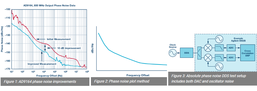 The simplest and most common test setup is shown in Figure 3. A clock source is used for the DDS and the DDS output is fed to a cross correlation type phase noise analyzer. This is easy to implement since only a single DDS is required. However, with this test setup, there is no method to extract the oscillator contribution to show only the DDS phase noise.
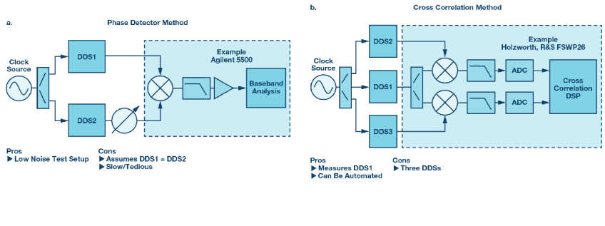
 The family of ultra low noise regulators with similar noise density is shown in Table 1. As demonstrated, the impact on the DAC phase noise is significant and these are also recommended for consideration for any areas of the RF system requiring optimum phase noise performance.
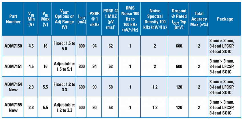
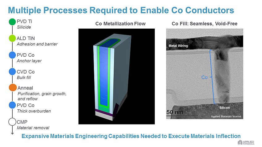 It includes: Applied Endura Cirrus RT PVD Cobalt To deposit the initial thin layer of cobalt to which the subsequent CVD cobalt adheres. Applied Endura Volta CVD Co to deposit the cobalt fill following the PVD layer. The seam created by this deposition process is subsequently eliminated during the anneal step. Applied Endura Versa XT PVD Co to deposit the thick overburden following the anneal step. Applied Producer Pyra Anneal to heats the wafer, causing cobalt reflow that eliminates the seam in the bulk fill, enlarges the grain size, purifies the cobalt, and reduces the resistance. Applied Reflexion LK Prime CMP: Using slurries specifically optimized for polishing cobalt, this system removes the overburden produced by earlier deposition steps and creates a planar surface for subsequent process steps.